


Afficheurs Lisibles Plein Soleil 12.3 pouces 1920x720 avec PCAP, LVDS
N° de modèle WF123BSWAYLNB0
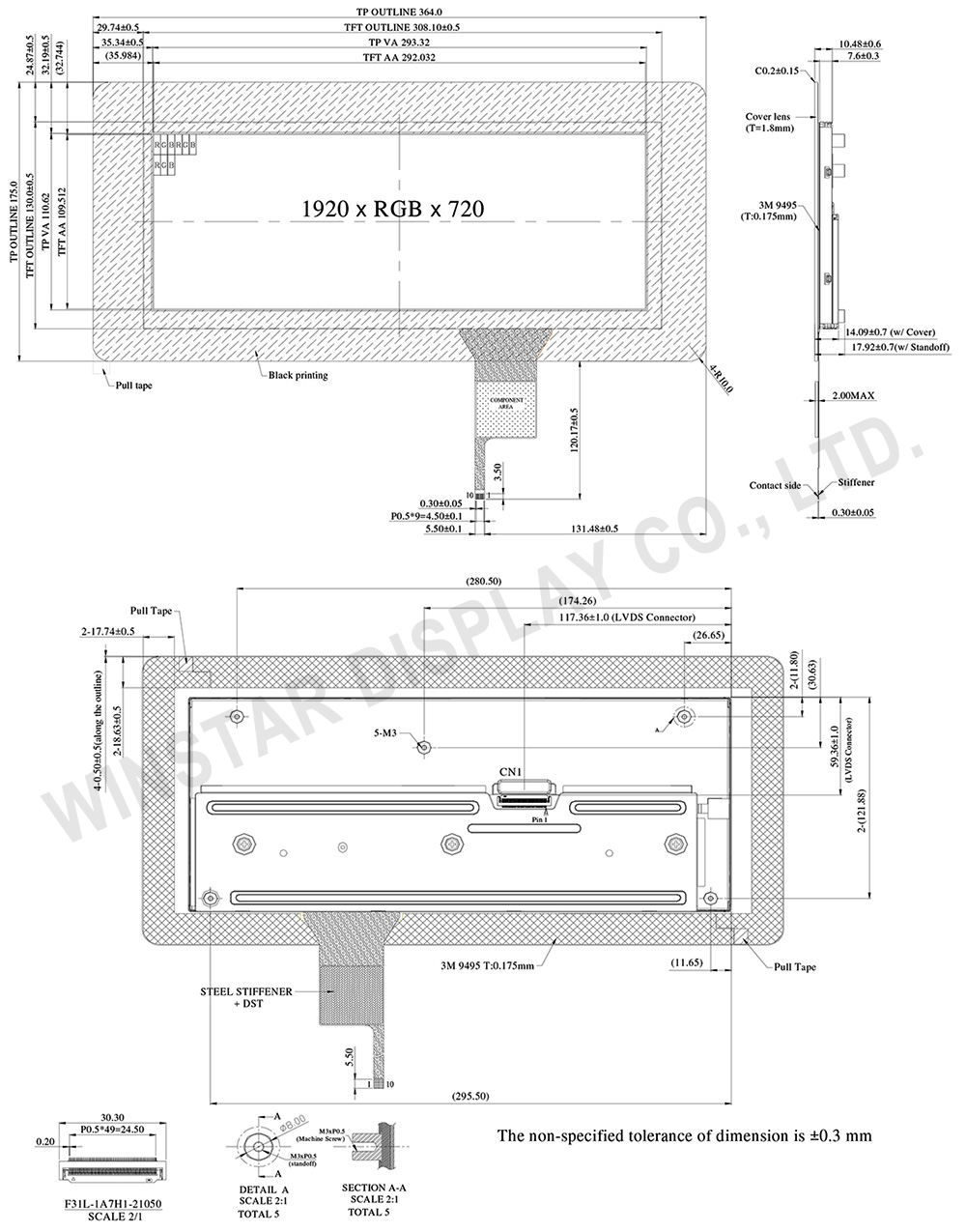
►Dimension: 12.3 pouces
►Résolution d’écran: 1920x720 points
►Vue préférentielle: 85/85/85/85 (IPS)
►Interface: 2ch-LVDS
►CI pilote: HX8298-C01-LT+HX8695-E-LT
►Carte de contrôle: NON
►Luminosité(cd/m²): 650
►Trou dans le cadre: NON
►Dalle tactile: Avec dalle tactile capacitive (PCAP)
►Detect Point: 10 Fingers
►Température d’utilisation: -30~+85℃
Description
The WF123BSWAYLNB0 is a 12.3-inch High Brightness TFT-LCD module with a resolution of 1920 x 720 pixels and an IPS panel, providing wide viewing angles of Left:85 / Right:85 / Up:85 / Down:85 degrees (typical value). It features a projected capacitive touch panel (PCAP) built-in with an ILI2511 IC, supporting both USB and I2C interfaces and accommodating up to 10 detect points.
This module supports a 2-ch LVDS (Low-Voltage-Differential-Signaling) interface, which is increasingly popular for larger TFT LCD displays. LVDS offers high-speed data transmission with low voltage, improved noise performance, and reduced susceptibility to EMI and crosstalk issues. It is particularly beneficial for peripherals requiring high bandwidth, such as high-definition graphics and fast frame rates, allowing for greater distance between the transmitting device and the display.
With a contrast ratio of 1100:1 (typical value) and a brightness of 650 nits (typical value), this TFT-LCD module ensures clear and vibrant display output. It features a glare surface panel and operates on a supply voltage (VCC) ranging from 3V to 3.6V, with a typical value of 3.3V. Additionally, it can withstand wide operating temperatures from -30℃ to +85℃ and storage temperatures from -40℃ to +85℃. For even wider storage temperature requirements (up to -40℃ to +90℃), the WF123BSWAYLNBA variant is available, albeit with a slightly thicker profile (10.7mm compared to 10.48mm).
DESSIN
SPÉCIFICATIONS
Fonction PIN sur l'interface
TFT LCD Module
FPC connector is used for electronics interface.
AORORA F31L-1A7H1-21050 , 50PIN
| Pin no. | Symbole | Fonction |
|---|---|---|
| 1 | GND | Ground |
| 2 | NC | No connector |
| 3 | VCC | Digital Power |
| 4 | VCC | Digital Power |
| 5 | GND | Panel Power |
| 6 | GND | Panel Power |
| 7 | NC | No connector |
| 8 | NC | No connector |
| 9 | GND | Ground |
| 10 | ORXIN0- | Odd pixel negative LVDS differential clock input |
| 11 | ORXIN0+ | Odd pixel positive LVDS differential clock input |
| 12 | ORXIN1- | Odd pixel negative LVDS differential clock input |
| 13 | ORXIN1+ | Odd pixel positive LVDS differential clock input |
| 14 | ORXIN2- | Odd pixel negative LVDS differential clock input |
| 15 | ORXIN2+ | Odd pixel positive LVDS differential clock input |
| 16 | ORXCLKIN- | Odd pixel negative LVDS differential clock input |
| 17 | ORXCLKIN+ | Odd pixel positive LVDS differential clock input |
| 18 | ORXIN3- | Odd pixel negative LVDS differential clock input |
| 19 | ORXIN3+ | Odd pixel positive LVDS differential clock input |
| 20 | ERXIN0- | Even pixel negative LVDS differential clock input |
| 21 | ERXIN0+ | Even pixel positive LVDS differential clock input |
| 22 | ERXIN1- | Even pixel negative LVDS differential clock input |
| 23 | ERXIN1+ | Even pixel positive LVDS differential clock input |
| 24 | ERXIN2- | Even pixel negative LVDS differential clock input |
| 25 | ERXIN2+ | Even pixel positive LVDS differential clock input |
| 26 | ERXCLKIN- | Even pixel negative LVDS differential clock input |
| 27 | ERXCLKIN+ | Even pixel positive LVDS differential clock input |
| 28 | ERXIN3- | Even pixel negative LVDS differential clock input |
| 29 | ERXIN3+ | Even pixel positive LVDS differential clock input |
| 30 | GND | Ground |
| 31 | NC | No connector |
| 32 | RESETB | Global reset pin, active low. |
| 33 | STBYB | Standby mode, active low. |
| 34 | CA3 | Output signal to indicate self protection mode, when DE,HS,VS,DCLK, any of these signals is missing, it will become High. If using this pin, CA3 need to pulled low by an resistor,else , let it floating. |
| 35 | SCL | Serial interface clock input. (User folating) |
| 36 | SDA | Serial interface data input/output.(User folating) |
| 37 | CSB | Serial interface chip enable.(User folating) |
| 38 | GND | Power Ground |
| 39 | GND | Power Ground |
| 40 | NC | No connector |
| 41 | LEDA | LED power (Anode) |
| 42 | LEDA | LED power (Anode) |
| 43 | LEDA | LED power (Anode) |
| 44 | NC | No connector |
| 45 | LEDK1 | Cathode 1 |
| 46 | LEDK2 | Cathode 2 |
| 47 | LEDK3 | Cathode 3 |
| 48 | LEDK4 | Cathode 4 |
| 49 | NTC_A | NTC_Anode |
| 50 | NTC_K | NTC_Cathode |
PCAP PIN Definition
| Pin | Symbole | Fonction |
|---|---|---|
| 1 | USB_VSS | System ground |
| 2 | USB_VDD 5V | Power supply |
| 3 | USB_D+ | Data + |
| 4 | USB_D- | Data - |
| 5 | VSS | System ground |
| 6 | SDA | I2C data input and output |
| 7 | SCL | I2C clock input |
| 8 | RST | External Reset, Low is active |
| 9 | INT | External interrupt to the host |
| 10 | VDDT 3.3 | Power supply |
Spécifications générales
| Article | Dimensions | Unité |
|---|---|---|
| Dimension | 12.3 | pouces |
| Pixel Number | 1920 RGB (H) × 720(V) | pixel |
| Dimensions du module | 364.0(H) × 175.0 (V) × 10.48 | mm |
| Zone active | 292.032(H) × 109.512(V) | mm |
| Pas des points | 0.1521(H) × 0.1521 (V) | mm |
| Type de LCD | TFT, Noir, Transmissif | |
| CI pilote | HX8298-C01-LT+HX8695-E-LT ou équivalent | |
| Angle de vue | 85/85/85/85 | |
| Type de rétroéclairage | LED, Blanc | |
| TFT Interface | 2ch-LVDS | |
| PCAP IC | ILI2511 ou équivalent | |
| PCAP Interface | USB (I2C available) | |
| Version PCAP FW | V6.0.0.0.0.0.0.3 | |
| Dalle tactile | Avec dalle tactile capacitive,PCA | |
| Surface | Reflets | |
Valeurs nominales maximales absolues
| Article | Symbole | Valeur min | Valeur type | Valeur max | Unité |
|---|---|---|---|---|---|
| Température de fonctionnement | TOP | -30 | - | +85 | ℃ |
| Température de stockage | TST | -40 | - | +85 | ℃ |
Caractéristiques électroniques
| Article | Symbole | Valeur min | Valeur type | Valeur max | Unité |
|---|---|---|---|---|---|
| Supply Voltage | VCC | 3 | 3.3 | 3.6 | V |
| Input signal voltage | ViH | VCC *0.7 | - | VCC | V |
| ViL | 0 | - | VCC *0.3 | V | |
| Current of power supply | ICC | - | - | 500 | mA |
| Inrush current | IRUSH | - | - | 2.0 | A |
| Supply PCAP (USB) | USB_VDD 5V | 4.75 | 5.0 | 5.25 | V |
| I USB_VDD | - | 90 | 135 | mA | |
| Supply PCAP (I2C) | VDDT 3.3 | 3.15 | 3.3 | 3.45 | V |
| IVDDT | - | 90 | 135 | mA |
