
- WEO012864U")
- WEO012864U")
- WEO012864U")
- WEO012864U")
2.7" SPI/ I2C 128x64 Органические светодиоды (Шкала серого)
Артикул. WEO012864U
►Тип: Графический
►Тип монтажа контроллера: COG
►Диагональ: 2.7 дюйма
►Разрешение: 128 x 64 точек
►IC:SSD1357
►3V Power supply
►1/64 duty
►Интерфейс: 6800, 8080, SPI, I2C
►Цвет дисплея: Белый / Желтый
►Инверсия
Описание
WEO012864U – 2.7'' дюймовый Графический COG OLED модуль с разрешением 128x64 точки c шлейфом для пайки. Дисплей WEO012832U сделан на базе контроллера IC SSD1315 c поддержкой интерфейсов: параллельного 6800/8080 8-Бит, I2C и четырехжильного SPI интерфейса. Напряжение питания 3V, а рабочий цикл 1/64.
OLED дисплей WEO012832U может работать в режиме полутонового изображения, которое имеет кодируемый 4 Бит канал яркости. Этот 2.7" -дюймовый OLED модуль идеально подходит для: настенных измерительных приборов, измерительных приборов промышленного применения, POS систем, Облачных/IoT систем, умных устройств, автомобилестроения, коммуникационных систем, медицинских устройств и т.д.
Аналогичные панели OLED также предлагаются в серии WEF012864U, которая включает в себя металлическую раму, исключая ППК, и серии WEP012864U, которая включает в себя как металлическую раму, так и ППК. Если вам требуется функциональность сенсорного экрана, рекомендуем рассмотреть возможность выбора серии WEP012864U-CTP.
Чертеж
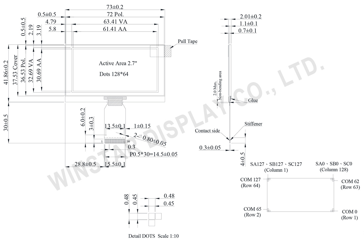
Data source ref:WEO012864UWPP3N00000
Технические характеристики
Функции контроллера контактного интерфейса
| No. | Символы | Описание | |||||||||||||||
|---|---|---|---|---|---|---|---|---|---|---|---|---|---|---|---|---|---|
| 1 | NC(GND) | No connection. | |||||||||||||||
| 2 | VSS | Ground of Logic Circuit. This is a ground pin. It also acts as a reference for the logic pins. It must be connected to external ground. |
|||||||||||||||
| 3 | VCC | Power supply for panel driving voltage. This is also the most positive power voltage supply pin. | |||||||||||||||
| 4 | VCOMH | Voltage Output High Level for COM Signal. This pin is the input pin for the voltage output high level for COM signals. A tantalum capacitor should be connected between this pin and VSS. |
|||||||||||||||
| 5 | VLSS | Ground of Analog Circuit These are the analog ground pins. They should be connected to VSS externally. |
|||||||||||||||
| 6~13 | D7~D0 | These pins are bi-directional data bus connecting to the MCU data bus. Unused pins are recommended to tie LOW. When serial interface mode is selected, D0 will be the serial clock input: SCLK; D1 will be the serial data input: SDIN and D2 should be kept NC. When I2C mode is selected, D2, D1 should be tied together and serve as SDAout, SDAin in application and D0 is the serial clock input, SCL. |
|||||||||||||||
| 14 | E/RD# | This pin is MCU interface input. When 6800 interface mode is selected, this pin will be used as the Enable (E) signal. Read/write operation is initiated when this pin is pulled HIGH and the chip is selected. When 8080 interface mode is selected, this pin receives the Read (RD#) signal. Read operation is initiated when this pin is pulled LOW and the chip is selected. When serial or I2C interface is selected, this pin must be connected to VSS. |
|||||||||||||||
| 15 | R/W# | This pin is read / write control input pin connecting to the MCU interface. When 6800 interface mode is selected, this pin will be used as Read/Write (R/W#) selection input. Read mode will be carried out when this pin is pulled HIGH and write mode when LOW. When 8080 interface mode is selected, this pin will be the Write (WR#) input. Data write operation is initiated when this pin is pulled LOW and the chip is selected. When serial or I2C interface is selected, this pin must be connected to VSS. |
|||||||||||||||
| 16 17 |
BS1 BS2 |
Communicating Protocol Select. These pins are MCU interface selection input. See the following table:
|
|||||||||||||||
| 18 | D/C# | This pin is Data/Command control pin connecting to the MCU. When the pin is pulled HIGH, the data at D[7:0] will be interpreted as data. When the pin is pulled LOW, the data at D[7:0] will be transferred to a command register. In I2C mode, this pin acts as SA0 for slave address selection. When 3-wire serial interface is selected, this pin must be connected to VSS. |
|||||||||||||||
| 19 | CS# | Chip Select This pin is the chip select input. The chip is enabled for MCU communication only when CS# is pulled low. |
|||||||||||||||
| 20 | RES# | This pin is reset signal input. When the pin is pulled LOW, initialization of the chip is executed. Keep this pin pull HIGH during normal operation. |
|||||||||||||||
| 21 | FR | Frame Frequency Triggering Signal This pin will send out a signal that could be used to identify the driver status. Nothing should be connected to this pin. It should be left open individually. |
|||||||||||||||
| 22 | IREF | This pin is the segment output current reference pin. IREF is supplied externally. |
|||||||||||||||
| 23 | N.C. | Reserved Pin The N.C. pin between function pins is reserved for compatible and flexible design. |
|||||||||||||||
| 24 | VDD | Power Supply for I/O Pin. This pin is a power supply pin of I/O buffer. It should be connected to VCI or external source. All I/O signal should have VIH reference to VDDIO. When I/O signal pins (BS0~BS1, D0~D7, control signals…) pull high, they should be connected to VDDIO. |
|||||||||||||||
| 25 | VP | Power Supply for Core Logic Circuit This is a voltage supply pin. It can be supplied externally (within the range of 2.4~2.6V) or regulated internally from VCI. A capacitor should be connected between this pin & VSS under all circumstances. |
|||||||||||||||
| 26 | VDD | Power Supply for Operation. This is a voltage supply pin. It must be connected to external source & always be equal to or higher than VDD & VDDIO. |
|||||||||||||||
| 27 | VSL | Voltage Output Low Level for SEG Signal This is segment voltage (output low level) reference pin. This pin has to connect with resistor and diode to ground (details depends on application). |
|||||||||||||||
| 28 | VLSS | Ground of Analog Circuit These are the analog ground pins. They should be connected to VSS externally. |
|||||||||||||||
| 29 | VCC | Power Supply for OEL Panel These are the most positive voltage supply pin of the chip. They must be connected to external source. |
|||||||||||||||
| 30 | NC(GND) | No connection |
Механические характеристики
| Наименование | Измерения | Единица |
|---|---|---|
| Разрешение | 128 x 64 | точек |
| Габариты | 73.0 × 41.86 × 2.01 | mm |
| Активная область | 61.41 × 30.69 | mm |
| Размер пикселя | 0.45 × 0.45 | mm |
| Шаг пикселя | 0.48 × 0.48 | mm |
| Матрица | Пассивная | |
| Цвет дисплея | монохромные | |
| Рабочий цикл | 1/64 Duty | |
| IC | SSD1357 | |
| Интерфейс | 6800, 8080, SPI, I2C | |
| Диагональ | 2.7 дюйма | |
Абсолютные максимальные значения
| Параметр | Символы | Минимальный | Максимальный | Единица |
|---|---|---|---|---|
| Supply Voltage for Logic | VDD | -0.3 | 4.0 | V |
| Supply Voltage for Display | VCC | 0 | 15.0 | V |
| Operating Temperature | TOP | -40 | 80 | °C |
| Storage Temperature | TSTG | -40 | 85 | °C |
Электронные характеристики
| Наименование | Символы | Кондиция | Минимальный | Типичный | Максимальный | Единица |
|---|---|---|---|---|---|---|
| Supply Voltage for Logic | VDD | - | 2.8 | 3.0 | 3.3 | V |
| Supply Voltage for Display | VCC | - | 9.5 | 10.0 | 10.5 | V |
| High Level Input | VIH | - | 0.8×VDD | - | - | V |
| Low Level Input | VIL | - | - | - | 0.2×VDD | V |
| High Level Output | VOH | - | 0.9×VDD | - | - | V |
| Low Level Output | VOL | - | - | - | 0.1×VDD | V |
| 50% Check Board operating Current | VCC =10.0V | - | 46 | 69 | mA | |
