
 - WO12864K1")
 - WO12864K1")
 - WO12864K1")
128x64 Графический COG LCD модуль (ST7565P, Positive Voltage)
Артикул. WO12864K1
►COG LCD дисплей 128x64
►Графический LCD
►IC: ST7565P
►3V power supply
►1/65 duty cycle, 1/9 bias
►Интерфейс : 6800/8080/SPI
Описание
WO12864K и WO12864K1 – монохромные символьные COG ЖК-модули с разрешением 128x64 пикселей. Данные дисплеи имеют встроенный ST7565 контроллер IC c поддержкой интерфейсов: параллельного 6800/8080 8-Бит и 4-х жильного SPI интерфейса. Напряжение питания дисплея 3V (напряжение под нагрузкой VOP – 9.5V), 1/65 рабочий цикл. Рабочая температура модуля: -20℃ до +70℃, с температурой хранения -30℃ to +80℃. В настоящее время дисплеи WO12864K / WO12864K1 доступны в варианте «негативный STN с синим трансмиссивным поляризатором и белой LED подсветкой. Если Вам нужна версия с подсветкой друого цвета, пожалуйста свяжитесь с нами.
WO12864K - версия с отрицательным напряжением (контроллер IC ST7565V)
WO12864K1 - версия с положительным напряжением (контроллер IC ST7565P)
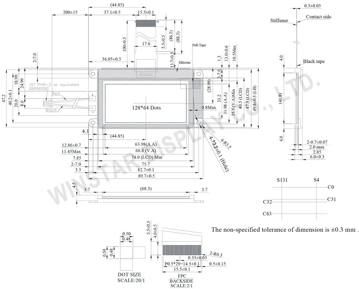
Чертеж
Data source ref: WO12864K1-TMI#
Технические характеристики
Функции контроллера контактного интерфейса
| Pin No. | Символы | Описание | |||||||||||||||
|---|---|---|---|---|---|---|---|---|---|---|---|---|---|---|---|---|---|
| 1 | /CS1 | This is the chip select signal. When /CS1 = “L” and CS2 = “H”, then the chip select becomes active, and data/command I/O is enabled. | |||||||||||||||
| 2 | /RES | When /RES is set to “L”, the register settings are initialized (cleared). The reset operation is performed by the /RES signal level. |
|||||||||||||||
| 3 | A0 | This is connect to the least significant bit of the normal MPU address bus, and it determines whether the data bits are data or command. A0 = “H”: Indicates that D0 to D7 are display data. A0 = “L”: Indicates that D0 to D7 are control data. |
|||||||||||||||
| 4 | /WR | • When connected to 8080 series MPU, this pin is treated as the “/WR” signal of the 8080 MPU and is LOW-active. The signals on the data bus are latched at the rising edge of the /WR signal. • When connected to 6800 series MPU, this pin is treated as the “R/W” signal of the 6800 MPU and decides the access type : When R/W = “H”: Read. When R/W = “L”: Write. |
|||||||||||||||
| 5 | /RD | • When connected to 8080 series MPU, this pin is treated as the “/RD” signal of the 8080 MPU and is LOW-active. The data bus is in an output status when this signal is “L”. • When connected to 6800 series MPU, this pin is treated as the “E” signal of the 6800 MPU and is HIGH-active. This is the enable clock input terminal of the 6800 Series MPU. |
|||||||||||||||
| 6 | D0 | This is an 8-bit bi-directional data bus that connects to an 8-bit or 16-bit standard MPU data bus. When the serial interface (SPI-4) is selected (P/S = “L”) : D7 : serial data input (SI) ; D6 : the serial clock input (SCL). D0 to D5 should be connected to VDD or floating. When the chip select is not active, D0 to D7 are set to high impedance. |
|||||||||||||||
| 7 | D1 | ||||||||||||||||
| 8 | D2 | ||||||||||||||||
| 9 | D3 | ||||||||||||||||
| 10 | D4 | ||||||||||||||||
| 11 | D5 | ||||||||||||||||
| 12 | D6 | ||||||||||||||||
| 13 | D7 | ||||||||||||||||
| 14 | VDD | Power supply Power supply | |||||||||||||||
| 15 | GND | Ground | |||||||||||||||
| 16 | VOUT | DC/DC voltage converter. Connect a capacitor between this terminal and VSS or VDD | |||||||||||||||
| 17 | CAP3+ | DC/DC voltage converter. Connect a capacitor between this terminal and the CAP1N terminal. | |||||||||||||||
| 18 | CAP1- | DC/DC voltage converter. Connect a capacitor between this terminal and the CAP1P terminal. | |||||||||||||||
| 19 | CAP1+ | DC/DC voltage converter. Connect a capacitor between this terminal and the CAP1N terminal. | |||||||||||||||
| 20 | CAP2+ | DC/DC voltage converter. Connect a capacitor between this terminal and the CAP2N terminal. | |||||||||||||||
| 21 | CAP2- | DC/DC voltage converter. Connect a capacitor between this terminal and the CAP2P terminal. | |||||||||||||||
| 22 | V4 | This is a multi-level power supply for the liquid crystal drive. The voltage Supply applied is determined by the liquid crystal cell, and is changed through the use of a resistive voltage divided or through changing the impedance using an op. amp. Voltage levels are determined based on Vss, and must maintain the relative magnitudes shown below. V0 ≧V1 ≧V2 ≧V3 ≧V4 ≧Vss When the power supply turns ON, the internal power supply circuits produce the V1 to V4 voltages shown below. The voltage settings are selected using the LCD bias set command. |
|||||||||||||||
| 23 | V3 | ||||||||||||||||
| 24 | V2 | ||||||||||||||||
| 25 | V1 | ||||||||||||||||
| 26 | V0 | ||||||||||||||||
| 27 | VR | Output voltage regulator terminal. Provides the voltage between VSS and V0 through a resistive voltage divider. IRS = “L” : the V0 voltage regulator internal resistors are not used. IRS = “H” : the V0 voltage regulator internal resistors are used. |
|||||||||||||||
| 28 | C86 | This is the MPU interface selection pin. C86 = “H”: 6800 Series MPU interface. C86 = “L”: 8080 Series MPU interface. | |||||||||||||||
| 29 | P/S | This pin configures the interface to be parallel mode or serial mode. P/S = “H”: Parallel data input/output. P/S = “L”: Serial data input. The following applies depending on the P/S status:
/RD (E) and /WR (R/W) are fixed to either “H” or “L”. The serial access mode does NOT support read operation. |
|||||||||||||||
| 30 | IRS | This terminal selects the resistors for the V0 voltage level adjustment. IRS = “H”: Use the internal resistors IRS = “L”: Do not use the internal resistors. The V0 voltage level is regulated by an external resistive voltage divider attached to the VR terminal |
Механические характеристики
| Наименование | Измерения | Единица |
|---|---|---|
| Разрешение | 128 x 64 | - |
| Габариты | 89.7 x 49.8 x 6.0 | mm |
| Видимая область | 66.8 x 35.5 | mm |
| Активная область | 63.98 x 31.98 | mm |
| Размер пикселя | 0.48 x 0.48 | mm |
| Шаг пикселя | 0.50x 0.50 | mm |
| Рабочий цикл | 1/65 duty , 1/9 Bias | |
| Тип подсветки | LED | |
| IC | ST7565P | |
Абсолютные максимальные значения
| Наименование | Символы | Минимальный | Типичный | Максимальный | Единица |
|---|---|---|---|---|---|
| Диапазон рабочих температур | TOP | -20 | - | +70 | ℃ |
| Температура хранения | TST | -30 | - | +80 | ℃ |
| Напряжение питания | VDD | -0.3 | - | 3.6 | V |
| Напряжение питания (VDD standard) | V0, VOUT | -0.3 | - | 14.5 | V |
| Напряжение питания (VDD standard) | V1, V2, V3, V4 | -0.3 | - | V0+0.3 | V |
Электронные характеристики
| Наименование | Символы | Stan | Минимальный | Типичный | Максимальный | Единица |
|---|---|---|---|---|---|---|
| Напряжение питания логических схем | VDD-VSS | - | 2.8 | 3.0 | 3.2 | V |
| Напряжение питания LCD | VOP | Ta=-20℃ Ta=25℃ Ta=70℃ |
- 9.3 - |
- 9.5 - |
- 9.7 - |
V V V |
| Высокое входное напряжение. | VIH | - | 0.8 VDD | - | VDD | V |
| Низкое входное напряжение | VIL | - | Vss | - | 0.2 VDD | V |
| Высокое напряжение на выходе | VOH | - | 0.8 VDD | - | VDD | V |
| Низкое напряжение на выходе | VOL | - | Vss | - | 0.2 VDD | V |
| Напряжение тока | IDD | VDD=3.0V | - | - | 2.0 | mA |
Search Keyword: lcd 128x64, lcd display 128x64, 128x64 lcd display
