


설명
도면
Data source ref: WEO012864ZLPP3N00000
사양
인터페이스 핀 기능
| Pin No. | 기호 | 기능 | ||||||
|---|---|---|---|---|---|---|---|---|
| 1 | VSS | Ground pin. | ||||||
| 2 | VCC | Power supply for panel driving voltage. This is also the most positive power voltage supply pin. | ||||||
| 3 | VCOMH | COM signal deselected voltage level. A capacitor should be connected between this pin and VSS. |
||||||
| 4 | VCI | Power supply pin for core logic operation | ||||||
| 5 | NC | No connection | ||||||
| 6 | BS1 | MCU bus interface selection pins. Select appropriate logic setting as described in the following table.
(1) 0 is connected to VSS (2) 1 is connected to VCI |
||||||
| 7 | IREF | This is segment output current reference pin. When external IREF is used, a resistor should be connected between this pin and VSS to maintain the IREF current at a maximum of 30uA. |
||||||
| 8 | CS# | This pin is the chip select input. (active LOW). | ||||||
| 9 | RES# | This pin is reset signal input. When the pin is pulled LOW, initialization of the chip is executed. Keep this pin HIGH during normal operation. |
||||||
| 10 | D/C# | When 4-wire serial interface is selected, this pin is Data/Command control pin connecting to the MCU. In I2C mode, this pin acts as SA0 for slave address selection. |
||||||
| 11 | D0 | These pins are bi-directional data bus connecting to the MCU data bus. When serial interface mode is selected, D0 will be the serial clock input: SCLK; D1 will be the serial data input: SDIN and D2 should be kept NC. When I2C mode is selected, D2, D1 should be tied together and serve as SDAout, SDAin in application and D0 is the serial clock input, SCL. |
||||||
| 12 | D1 | |||||||
| 13 | D2 | |||||||
| 14 | NC | No connection | ||||||
| 15 | NC | No connection | ||||||
| 16 | NC | No connection | ||||||
| 17 | VCC | Power supply for panel driving voltage. This is also the most positive power voltage supply pin. | ||||||
| 18 | VSS | Ground pin. |
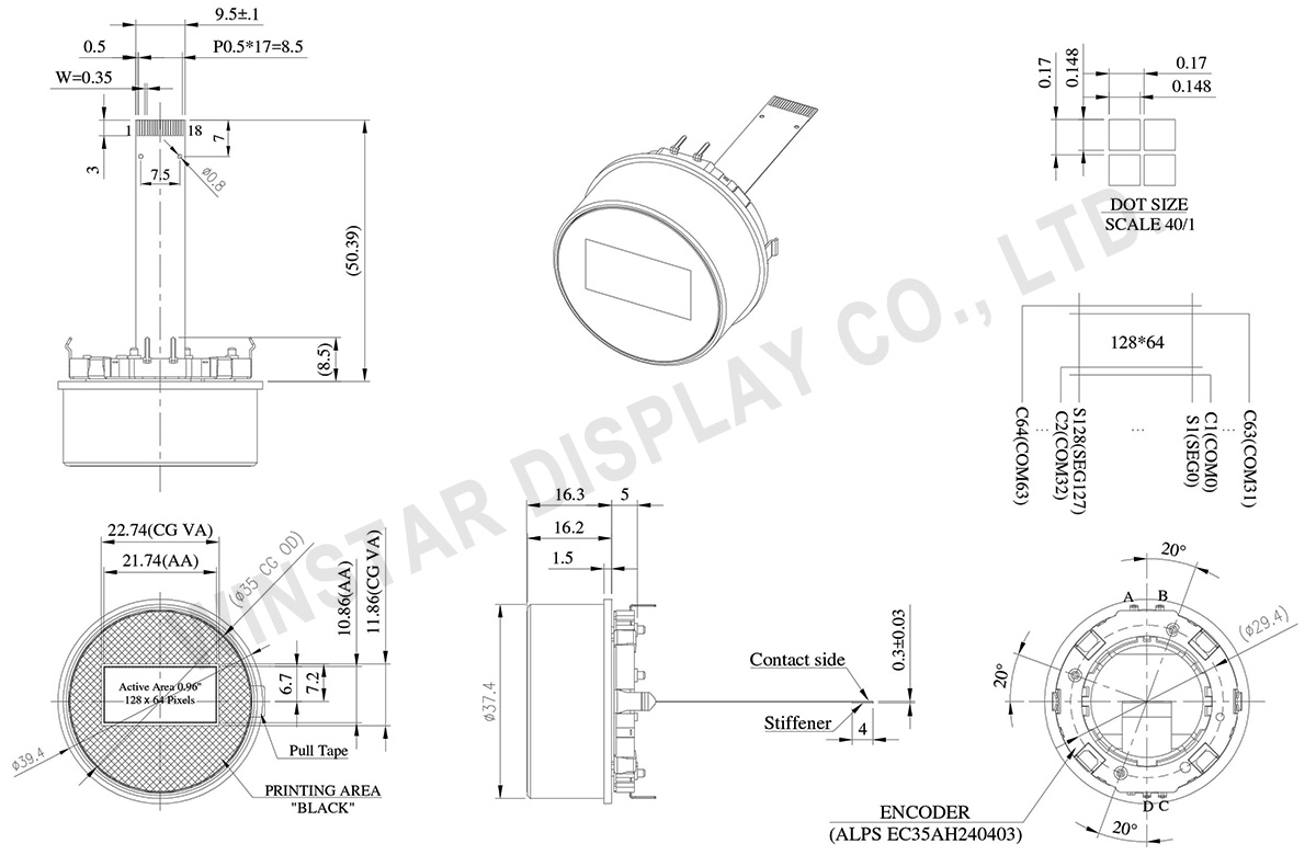
Encoder PIN Definition
| No. | 기호 | 기능 |
|---|---|---|
| 1 | FSW_A | Encoder terminal signal-A |
| 2 | FSW_B | Encoder terminal signal-B |
| 3 | FSW_C | Encoder terminal signal-C |
| 4 | FSW_D | Ground |
기계적 데이터
| 항목 | 치수 | 단위 |
|---|---|---|
| 도트 매트릭스 | 128 x 64 | Dots |
| 모듈 치수 | Ø39.4 x 24.8 | mm |
| 활성 영역 | 21.74 x 10.86 | mm |
| 도트 크기 | 0.148 x 0.148 | mm |
| 도트 피치 | 0.17 x 0.17 | mm |
| 디스플레이 모드 | 패시브 매트릭스 (Passive Matrix) | |
| 디스플레이 색 | Monochrome | |
| Drive Duty | 1/64 | |
| IC | SSD1326 | |
| 인터페이스 | 4-line SPI , I2C | |
| 크기 (대각선) | 0.96 인치 | |
절대 최대 정격값
| 항목 | 기호 | 최소값 | 최대값 | 단위 |
|---|---|---|---|---|
| Supply Voltage | VCI | -0.3 | 4.0 | V |
| Supply Voltage for Display | VCC | 0 | 15 | V |
| 작동 온도 | TOP | -20 | +70 | °C |
| 보관 온도 | TST | -30 | +80 | °C |
전기적 특성
DC 전기적 특성
| 항목 | 기호 | 조건 | 최소값 | 대표값 | 최대값 | 단위 |
|---|---|---|---|---|---|---|
| Supply Voltage | VCI | - | 1.65 | 3.0 | 3.3 | V |
| Supply Voltage for Display | VCC | - | 6 | 10 | 10.5 | V |
| Input High Volt. | VIH | - | 0.8xVCI | - | - | V |
| Input Low Volt. | VIL | - | - | - | 0.2xVCI | V |
| Output High Volt. | VOH | Iout = 100uA | 0.9xVCI | - | - | V |
| Output Low Volt. | VOL | Iout = 100uA | - | - | 0.1xVCI | V |
| Operating Current for VCC (VCC Supplied Externally) | ICC | VCC =10V | - | 5 | 10 | mA |
Search keyword: 128x64 oled, oled 128x64, 0.96 oled, 0.96" oled, 0.96 인치 oled, oled 0.96"
