


설명

도면
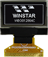
WEO012864C with Hotbar FPC
Data source ref: WEO012864CWAP3N00001
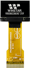
WEO012864C with ZIF FPC
사양
인터페이스 핀 기능
| No. | 기호 | 기능 | |||||||||||||||
|---|---|---|---|---|---|---|---|---|---|---|---|---|---|---|---|---|---|
| 1 | NC | No connection | |||||||||||||||
| 2 | C1N | Connect to charge pump capacitor. These pins are not used and should be disconnected when Vpp is supplied externally. |
|||||||||||||||
| 3 | C1P | ||||||||||||||||
| 4 | C2P | Connect to charge pump capacitor. These pins are not used and should be disconnected when Vpp is supplied externally. |
|||||||||||||||
| 5 | C2N | ||||||||||||||||
| 6 | VDD2 | 3.0 – 4.7V power supply pad for Power supply for charge pump circuit. This pin should be disconnected when VPP is supplied externally |
|||||||||||||||
| 7 | NC | No connection | |||||||||||||||
| 8 | VSS | Ground. | |||||||||||||||
| 9 | VDD1 | Power supply input: 1.65 - 3.5V | |||||||||||||||
| 10 | NC | No connection | |||||||||||||||
| 11 | IM1 | These are the MPU interface mode select pads.
|
|||||||||||||||
| 12 | IM2 | ||||||||||||||||
| 13 | CSB | This pad is the chip select input. When CSB = “L”, then the chip select becomes active, and data/command I/O is enabled. | |||||||||||||||
| 14 | RESB | This is a reset signal input pad. When RES is set to “L”, the settings are initialized. The reset operation is performed by the RES signal level. | |||||||||||||||
| 15 | A0 | This is the Data/Command control pad that determines whether the data bits are data or a command. A0 = “H”: the inputs at D0 to D7 are treated as display data. A0 = “L”: the inputs at D0 to D7 are transferred to the command registers. In I2C interface, this pad serves as SA0 to distinguish the different address of OLED driver. |
|||||||||||||||
| 16 | WRB | This is a MPU interface input pad. When connected to an 8080 MPU, this is active LOW. This pad connects to the 8080 MPU WR signal. The signals on the data bus are latched at the rising edge of the WR signal. When connected to a 6800 Series MPU: This is the read/write control signal input terminal. When R/W = “H”: Read. When R/W = “L”: Write. |
|||||||||||||||
| 17 | RDB | This is a MPU interface input pad. When connected to an 8080 series MPU, it is active LOW. This pad is connected to the RD signal of the 8080 series MPU, and the data bus is in an output status when this signal is “L”. When connected to a 6800 series MPU , this is active HIGH. This is used as an enable clock input of the 6800 series MPU. When RD = “H”: Enable. When RD = “L”: Disable. |
|||||||||||||||
| 18 | D0 | This is an 8-bit bi-directional data bus that connects to an 8-bit or 16-bit standard MPU data bus. When the serial interface is selected, then D0 serves as the serial clock input pad (SCL) and D1 serves as the serial data input pad (SI). At this time, D2 to D7 are set to high impedance. When the I2C interface is selected, then D0 serves as the serial clock input pad (SCL) and D1 serves as the serial data input pad (SDAI). At this time, D2 to D7 are set to high impedance. |
|||||||||||||||
| 19 | D1 | ||||||||||||||||
| 20 | D2 | ||||||||||||||||
| 21 | D3 | ||||||||||||||||
| 22 | D4 | ||||||||||||||||
| 23 | D5 | ||||||||||||||||
| 24 | D6 | ||||||||||||||||
| 25 | D7 | ||||||||||||||||
| 26 | IREF | This is a segment current reference pad. A resistor should be connected between this pad and VSS. Set the current at 18.75uA. | |||||||||||||||
| 27 | VCOMH | This is a pad for the voltage output high level for common signals. A capacitor should be connected between this pad and VSS. |
|||||||||||||||
| 28 | VPP | OLED panel power supply. Generated by internal charge pump. Connect to capacitor. It could be supplied externally. |
|||||||||||||||
| 29 | NC | No connection | |||||||||||||||
| 30 | NC | No connection |
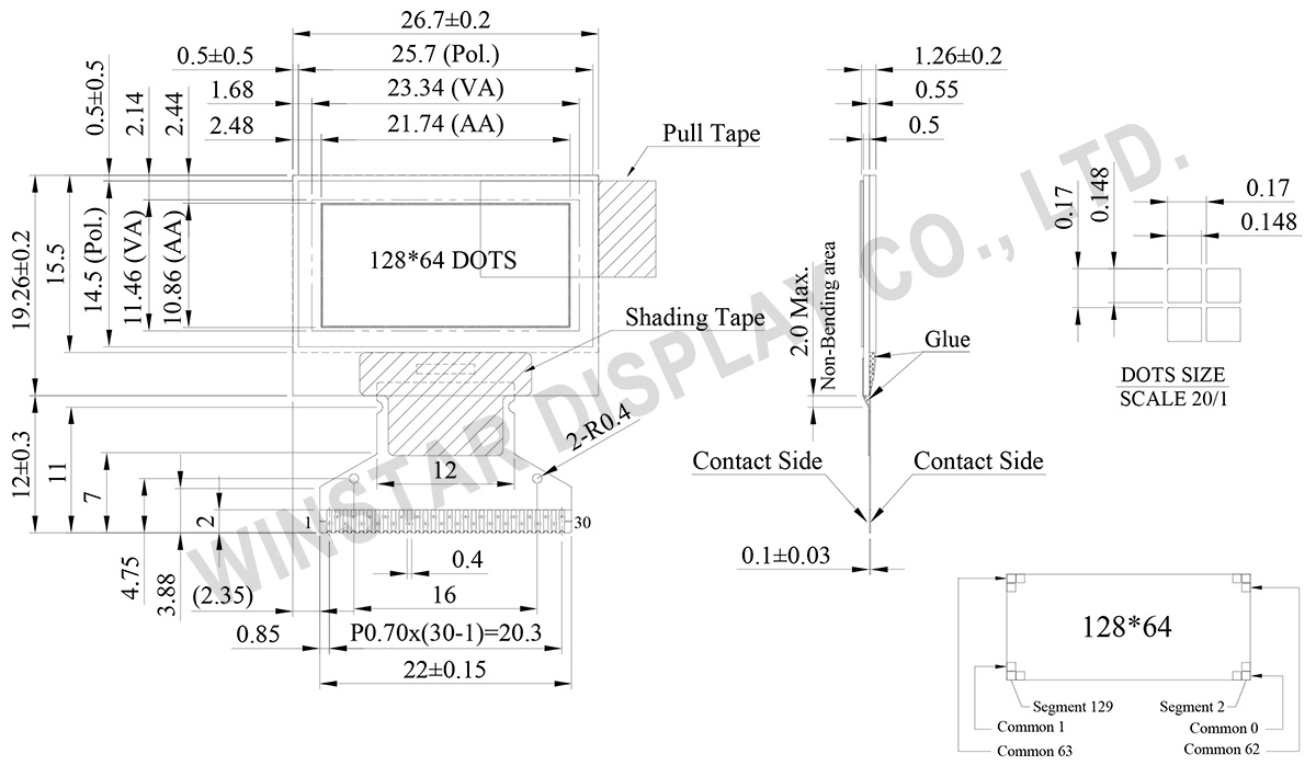
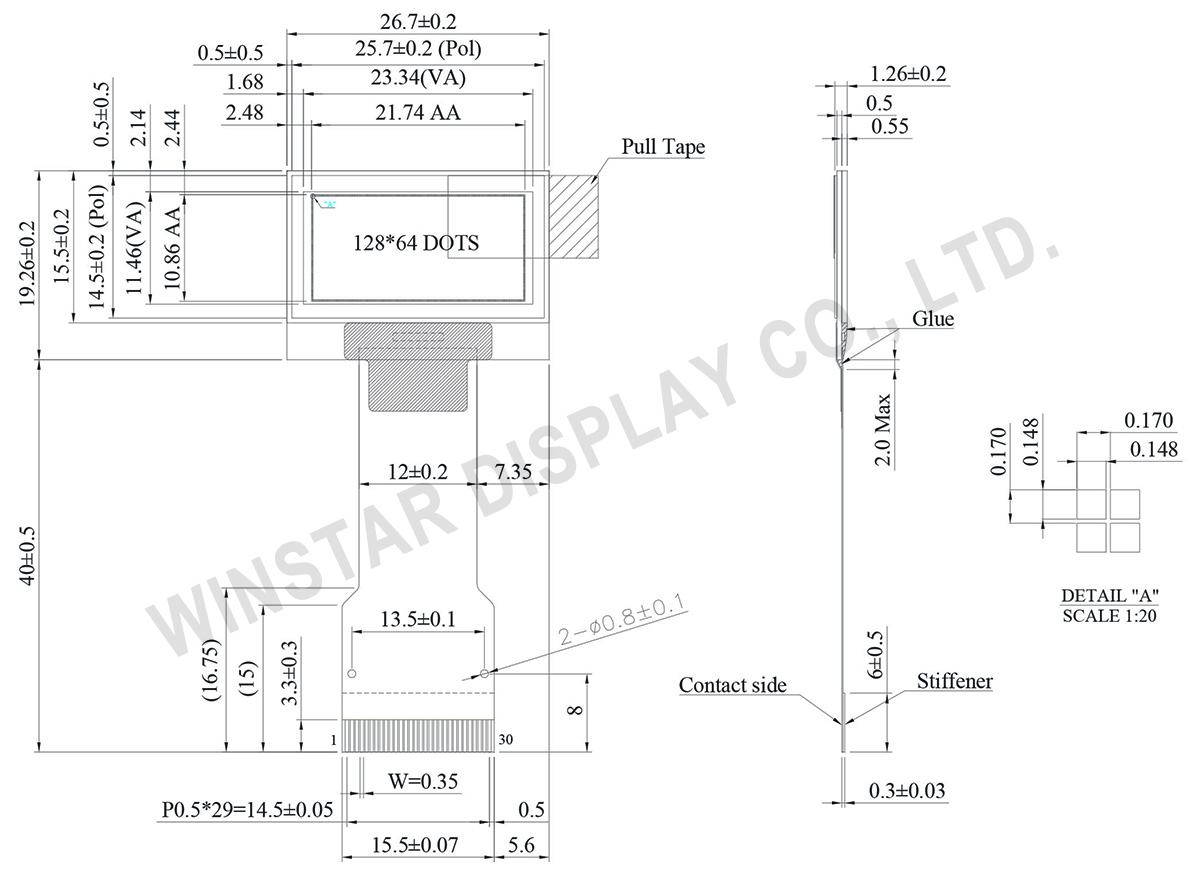
일반 사양
| 항목 | 치수 | 단위 |
|---|---|---|
| 도트 매트릭스 | 128 x 64 | - |
| 모듈 치수 | 26.70 × 19.26 ×1.26 | mm |
| 활성 영역 | 21.74 × 10.86 | mm |
| 도트 크기 | 0.148 × 0.148 | mm |
| 도트 피치 | 0.170 × 0.170 | mm |
| 디스플레이 모드 | 패시브 매트릭스 | |
| 디스플레이 색상 | Monochrome | |
| Drive Duty | 1/64 Duty | |
| 제어 IC | SH1106 | |
| 인터페이스 | 6800, 8080, SPI, I2C | |
| 크기 | 0.96 인치 | |
절대 최대 정격값
| Parameter | 기호 | 최소값 | 최대값 | 단위 |
|---|---|---|---|---|
| Supply Voltage for Logic | VDD1 | -0.3 | 3.6 | V |
| Power supply for charge pump circuit | VDD2 | -0.3 | 4.8 | V |
| Supply Voltage for Display | VPP | -0.3 | 14.5 | V |
| 작동 온도 | TOP | -40 | +80 | °C |
| 보관 온도 | TSTG | -40 | +85 | °C |
전기적 특성
DC 전기적 특성
| 항목 | 기호 | 조건 | 최소값 | 대표값 | 최대값 | 단위 |
|---|---|---|---|---|---|---|
| Supply Voltage for Logic | VDD1 | - | 2.8 | 3.0 | 3.3 | V |
| Power supply for charge pump circuit | VDD2 | - | 3.5 | 3.8 | 4.2 | V |
| Charge Pump Output Voltage for Display (Generated by Internal DC/DC) |
Charge Pump VPP |
- | 7.5 | 8 | 8.5 | V |
| High Level Input | VIH | - | 0.8xVDD1 | - | VDD1 | V |
| Low Level Input | VIL | - | VSS | - | 0.2xVDD1 | V |
| High Level Output | VOH | - | 0.8xVDD1 | - | VDD1 | V |
| Low Level Output | VOL | - | VSS | - | 0.2xVDD1 | V |
| Operating Current for VDD2 Display 50% ON | IDD2 | - | - | 10 | 16 | mA |
FPC 옵션:
| 그림 | FPC Length | PIN | Pitch | ZIF FPC or HOTBAR FPC | 인터페이스 | FPC No. | Create Date |
|---|---|---|---|---|---|---|---|
 |
13 | 30 | 0.7 | HOTBAR FPC | 6800, 8080, 4-Wire SPI, I2C | FPC2070003001XXXXX09 | 20180613 |
 |
40.95 | 30 | 0.5 | ZIF | 6800, 8080, SPI, I2C | FPC2050003011XXXXX23 | 20190412 |
Search keyword: 128x64 oled, oled 128x64, 0.96 oled, 0.96" oled, 0.96 인치 oled, oled 0.96, oled 0.96"
