


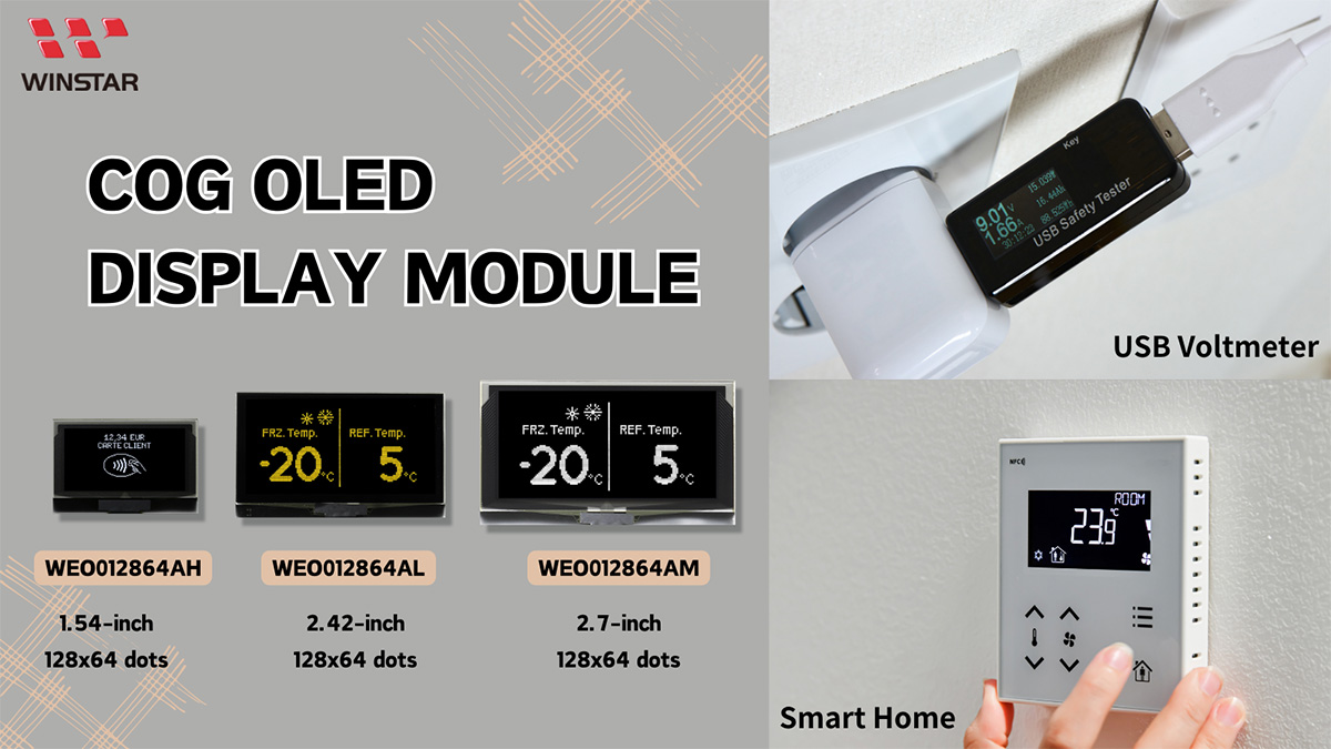
Moduli Display OLED COG 2.7 pollici Grafici 128x64
Modello numero WEO012864AM
►Tipo: grafico
►Struttura: COG
►Dimensione: 2.7 pollici
►128 x 64 a matrice di punti
►IC:SH1106
►Alimentatore 3V
►1/64 duty
►IInterfaccia: 6800,8080,4-wire SPI,I2C
►Colore display: Bianco / Giallo
Descrizione
WEO012864AM è un display OLED grafico COG da 2,7 pollici con risoluzione 128x64. Questo modulo è integrato con l'IC SH1106; può essere comunicato tramite interfaccia I2C, seriale SPI a 4 fili o interfaccia parallela 6800, 8080 e il suo alto rapporto di contrasto di 10.000: 1 rende l'immagine del display più chiara. La tensione di alimentazione della logica è compresa tra 1,65 V e 3,3 V (valore tipico 3V), la tensione di alimentazione per il display è compresa tra 6,4V e 13,5V (valore tipico 13V), duty di guida 1/64.
Questo modulo può funzionare a temperature da -40°C a +80°C; le temperature di stoccaggio vanno da -40°C a +85°C. Il display OLED da 2,7 pollici è molto adatto per applicazioni smart home, attrezzature hi-tech, apparecchiature di misurazione, sistemi di controllo industriale, strumenti medici, sistemi IoT...ecc. La serie WEO12864AM dispone di diversi connettori FPC ZIF; attualmente forniamo opzioni da 22 pin, 24 pin, 30 pin e 31 pin; se i clienti richiedono un FPC personalizzato, non esitate a contattarci.
DISEGNO
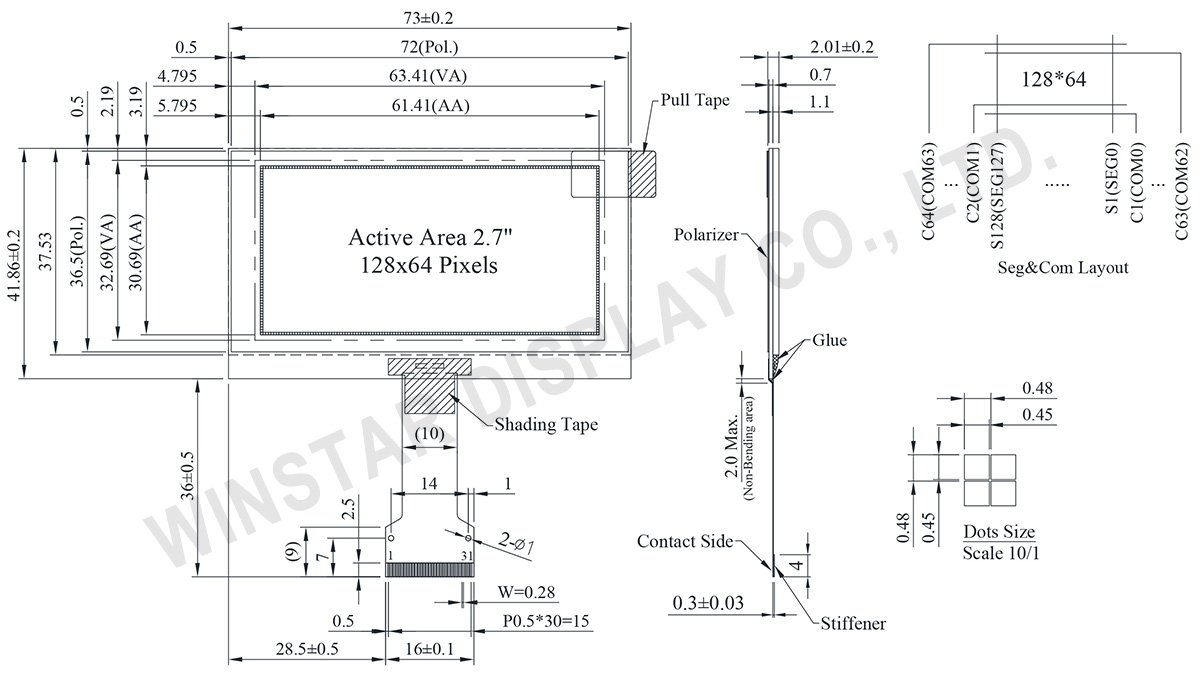
Data source ref:WEO012864AMWPP3N00000
SPECIFICHE TECNICHE
Funzione dei Pin di Interfaccia
| No. | Simbolo | Funzione | |||||||||||||||
|---|---|---|---|---|---|---|---|---|---|---|---|---|---|---|---|---|---|
| 1 | ESD_GND | ESD Ground pin | |||||||||||||||
| 2 | VSS | Ground. | |||||||||||||||
| 3-10 | NC | No connection | |||||||||||||||
| 11 | VDD1 | Power supply input | |||||||||||||||
| 12 | IM1 | These are the MPU interface mode select pads.
(1) 0 is connected to VSS (2) 1 is connected to VDD1 |
|||||||||||||||
| 13 | IM2 | ||||||||||||||||
| 14 | NC | No connection | |||||||||||||||
| 15 | /CS | This pad is the chip select input. When /CD = “L”, then the chip select becomes active, and data/command I/O is enabled. | |||||||||||||||
| 16 | /RES | This is a reset signal input pad. When /RES is set to “L”, the settings are initialized. The reset operation is performed by the /RES signal level. | |||||||||||||||
| 17 | A0 | This is the Data/Command control pad that determines whether the data bits are data or a command. A0 = “H”: the inputs at D0 to D7 are treated as display data. A0 = “L”: the inputs at D0 to D7 are transferred to the command registers. In I2C interface, this pad serves as SA0 to distinguish the different address of OLED driver. |
|||||||||||||||
| 18 | /WR (R/W) |
This is a MPU interface input pad. When connected to an 8080 MPU, this is active LOW. This pad connects to the 8080 MPU /WR signal. The signals on the data bus are latched at the rising edge of the /WR signal. When connected to a 6800 Series MPU: This is the read/write control signal input terminal. When R/W= “H”: Read. When R/W= “L”: Write. |
|||||||||||||||
| 19 | E/RD | This is a MPU interface input pad. When connected to an 8080 series MPU, it is active LOW. This pad is connected to the /RD signal of the 8080 series MPU, and the data bus is in an output status when this signal is “L”. When connected to a 6800 series MPU, this is active HIGH. This is used as an enable clock input of the 6800 series MPU. When /RD = “H”: Enable. When /RD = “L”: Disable. |
|||||||||||||||
| 20~27 | D0~D7 | This is an 8-bit bi-directional data bus that connects to an 8-bit or 16-bit standard MPU data bus. When the serial interface is selected, then D0 serves as the serial clock input pad (SCL) and D1 serves as the serial data input pad (SI). At this time, D2 to D7 are set to high impedance. When the I2C interface is selected, then D0 serves as the serial clock input pad (SCL) and D1 serves as the serial data input pad (SDAI). At this time, D2 to D7 are set to high impedance. |
|||||||||||||||
| 28 | IREF | This is a segment current reference pad. A resistor should be connected between this pad and VSS. Set the current at 18.75uA. | |||||||||||||||
| 29 | VCOMH | This is a pad for the voltage output high level for common signals. A capacitor should be connected between this pad and VSS. |
|||||||||||||||
| 30 | VPP | OLED panel power supply. Generated by internal charge pump. Connect to capacitor. It could be supplied externally. |
|||||||||||||||
| 31 | ESD_GND | ESD Ground pin |
Dati meccanici
| Articolo | Dimensioni | Unità |
|---|---|---|
| A matrice di punti | 128 × 64 | - |
| Dimensione del modulo | 73.0 × 41.86 × 2.01 | mm |
| Area attiva | 61.41 × 30.69 | mm |
| Dimensioni del Dot | 0.45 × 0.45 | mm |
| Passo del Dot | 0.48 × 0.48 | mm |
| Modalità display | Matrice passiva | |
| Colore display | Monocromatici | |
| Drive Duty | 1/64 Duty | |
| IC | SH1106 | |
| Interfaccia | 6800,8080,4-Wire SPI,I2C | |
| Dimensione (Diagonale) | 2.7 pollici | |
Valori massimi assoluti
| Parameter | Simbolo | Valore Min | Valore massimo | Unità |
|---|---|---|---|---|
| Supply Voltage for Logic | VDD1 | -0.3 | 3.6 | V |
| Supply Voltage for Display | VPP | -0.3 | 14.5 | V |
| Temperatura di lavoro | TOP | -40 | +80 | °C |
| Temperatura di stock | TSTG | -40 | +85 | °C |
Caratteristiche elettriche
| Articolo | Simbolo | Condizione | Valore Min | Valore tipico | Valore massimo | Unità |
|---|---|---|---|---|---|---|
| Supply Voltage for Logic | VDD1 | - | 1.65 | 3.0 | 3.3 | V |
| Supply Voltage for Display | VPP | - | 6.4 | 13.0 | 13.5 | V |
| High Level Input | VIH | - | 0.8×VDD1 | - | VDD1 | V |
| Low Level Input | VIL | - | VSS | - | 0.2×VDD1 | V |
| High Level Output | VOH | - | 0.8×VDD1 | - | VDD1 | V |
| Low Level Output | VOL | - | VSS | - | 0.2×VDD1 | V |
| Display 50% Pixel on | IPP | VPP =13V | - | 24 | 36 | mA |
Search keyword: 128x64 oled, oled 128x64, 2.7 oled, 2.7" oled, 2.7 pollici oled, oled 2.7, oled 2.7"
