


Écran IPS MIPI TFT 10,1 pouces 1024x600 Haute Luminosité avec PCAP
N° de modèle WF101JSYAHMNB0
►Dimension 10.1 pouces
►Résolution d’écran: 1024×600 points
►Vue préférentielle IPS
►Interface: MIPI DSI
►CI pilote : EK79007AD3+EK73217BCGA
►Carte de contrôle: No
►Luminosité (Cd/m²): 900
►Cadre de maintien avec points de fixation: NON
►Dalle tactile: Avec dalle tactile capacitive (PCAP)
►Detect Point : 5 Fingers
Description
The WF101JSYAHMNB0 is a 10.1-inch MIPI DSI interface High Brightness TFT-LCD module with a resolution of 1024 x 600 pixels and an IPS panel, offering wide viewing angles of Left:85 / Right:85 / Up:85 / Down:85 degrees (typical). It boasts a high brightness of 900 nits (typical value).
Featuring EK79007AD3 and EK73217BCGA driver ICs, this module supports 4-Lanes MIPI DSI interface. Additionally, it comes with a projected capacitive touch panel (PCAP) built-in with an ILI2511 IC, supporting both USB and I2C interfaces.
The MIPI DSI interface is renowned for its High Speed Data Transmission and High Speed Clock Transmission characteristics, enhancing performance. With a glare surface panel and an aspect ratio of 16:9, this TFT display module can operate reliably in temperatures ranging from -20℃ to +70℃, with storage temperatures from -30℃ to +80℃.
DESSIN
SPÉCIFICATIONS
Interface
TFT LCD Module
| Pin No. | Symbole | Function |
|---|---|---|
| 1 | VLED+ | LED Anode |
| 2 | VLED+ | LED Anode |
| 3 | VGH | Positive power for TFT |
| 4 | VGL | Negative power for TFT |
| 5 | UPDN | Gate up or down scan control. UPDN = ”L”, STV2 output vertical start pulse and UD pin output logical “L” to Gate driver. (default) UPDN = ”H”, STV1 output vertical start pulse and UD pin output logical “H” to Gate driver |
| 6 | SHLR | Source right or left sequence control. SHLR = ”L“, shift left: last data = S1←S2←S3….......←S1536 = first data. SHLR = ”H“, shift right: first data = S1→S2→S3….....→S1536 = last data.(default) |
| 7 | VLED- | LED Cathode |
| 8 | VLED- | LED Cathode |
| 9 | AVDD | Analog power |
| 10 | GND | Digital ground |
| 11 | D3P | MIPI data input. |
| 12 | D3N | MIPI data input. |
| 13 | GND | Digital ground |
| 14 | D2P | MIPI data input. |
| 15 | D2N | MIPI data input. |
| 16 | GND | Digital ground |
| 17 | CLKP | MIPI clock input |
| 18 | CLKN | MIPI clock input |
| 19 | GND | Digital ground |
| 20 | D1P | MIPI data input. |
| 21 | D1N | MIPI data input. |
| 22 | GND | Digital ground |
| 23 | D0P | MIPI data input. |
| 24 | D0N | MIPI data input. |
| 25 | GND | Digital ground |
| 26 | STBYB | Standby mode. STBYB = ”H“,normal operation(default) STBYB = ”L”, timing controller, source driver will turn off, all output are GND. |
| 27 | RESET | Global reset pin. Active Low to enter Reset State. Normally pull high. Connecting with an RC reset circuit for stability. |
| 28 | VDD (1.8V) | Digital power |
| 29 | VDD (1.8V) | Digital power |
| 30 | VCOMI | Common voltage |
PCAP PIN Definition
| Pin | Symbole | Function |
|---|---|---|
| 1 | USB_VSS | System ground |
| 2 | USB_VDD 5V | Power supply |
| 3 | USB_D+ | Data + |
| 4 | USB_D- | Data - |
| 5 | VSS | System ground |
| 6 | SDA | I2C data input and output |
| 7 | SCL | I2C clock input |
| 8 | RST | External Reset, Low is active |
| 9 | INT | External interrupt to the host |
| 10 | VDDT 3.3 | Power supply |
Spécifications générales
| Article | Dimensions | Unité |
|---|---|---|
| Screen Diagonal | 10.1 | pouce |
| Number of Pixels | 1024 RGB x 600 | points |
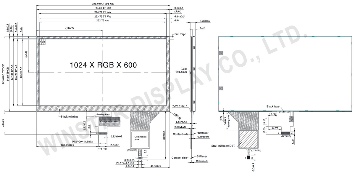
| Dimensions du module | 235(W) x 143(H) x 8.78(D) | mm |
| Zone active | 222.72 (H) x 125.28(V) | mm |
| Pixel pitch | 0.2175(W) x 0.2088(H) | mm |
| Type de LCD | TFT, Noir, Transmissif | |
| Interface | 4-Lanes MIPI | |
| CI pilote | EK79007AD3 + EK73217BCGA ou équivalent | |
| Vue préférentielle | 85/85/85/85 | |
| Rapport d'aspect | 16:9 | |
| Type de rétroéclairage | LED, Blanc | |
| PCAP IC | ILI2511 ou équivalent | |
| PCAP Interface | USB (I2C available) | |
| PCAP FW Version | V6.0.0.0.62.90.1.2 | |
| Avec/sans dalle tactile | Avec dalle tactile capacitive,PCAP | |
| Surface | Reflets | |
Valeurs nominales maximales absolues
| Article | Symbole | Min | Typ | Max | Unité |
|---|---|---|---|---|---|
| Température de fonctionnement | TOP | -20 | - | +70 | ℃ |
| Température de stockage | TST | -30 | - | +80 | ℃ |
Caractéristiques électroniques
Typical Operation Conditions (At Ta = 25 °C,)
| Article | Symbole | Min | Typ | Max | Unité |
|---|---|---|---|---|---|
| Digital Power Supply Voltage For LCD | VDD | 1.71 | 1.8 | 1.89 | V |
| Analog Power Supply Voltage | AVDD | 9.89 | 10.2 | 10.5 | V |
| Gate On Power Supply Voltage | VGH | 19.4 | 20.0 | 20.6 | V |
| Gate Off Power Supply Voltage | VGL | -10.3 | -10.0 | -9.7 | V |
| Common Power Supply Voltage | VCOMI | 4.0 | 4.3 | 4.6 | V |
| Supply PCAP | VDDT | 3.0 | 3.3 | 3.6 | V |
| IVDDT | 90.5 | 115 | mA | ||
| USB_VDD 5V | 4.4 | 5.0 | 5.5 | V | |
| I VDD 5V | — | 97.8 | 120 | mA |
