


2 lignes de 20 caractères COG Afficheurs OLED +PCB
N° de modèle WEA002002A
►Type : Alphanumérique
►Structure : COG+PCB
►2 lignes de 20 caractères
►IC:SSD1311
►Alimentation 3.3V
►1/16 duty
►Interface: 6800, 8080, SPI, I2C
►Couleur d'affichage: Blanc / Jaune
DESSIN
SPÉCIFICATIONS
Fonction PIN sur l'interface
| Pin No. | Symbole | Pin Type | Description | ||||||||||||||||||
|---|---|---|---|---|---|---|---|---|---|---|---|---|---|---|---|---|---|---|---|---|---|
| 1 | VSS | P | Ground pin. It must be connected to external ground. | ||||||||||||||||||
| 2 | VDD | P | Power supply for core logic operation. A capacitor should be connected between VDD and VSS under all circumstances. |
||||||||||||||||||
| 3 | REGVDD | I | Internal VDD regulator selection pin It must be connected to external ground. |
||||||||||||||||||
| 4 | D/C# | I | This pin is Data/Command control pin connecting to the MCU. When the pin is pulled HIGH, the data at D[7:0] will be interpreted as data. When the pin is pulled LOW, the data at D[7:0] will be transferred to a command register. In I2C mode, this pin acts as SA0 for slave address selection. When serial interface is selected, this pin must be connected to VSS. |
||||||||||||||||||
| 5 | R/W# | I | This pin is read / write control input pin connecting to the MCU interface. When 6800 interface mode is selected, this pin will be used as Read/Write (R/W#) selection input. Read mode will be carried out when this pin is pulled HIGH and write mode when LOW. When 8080 interface mode is selected, this pin will be the Write (WR#) input. Data write operation is initiated when this pin is pulled LOW and the chip is selected. When serial or I2C interface is selected, this pin must be connected to VSS. |
||||||||||||||||||
| 6 | E | I | This pin is MCU interface input. When 6800 interface mode is selected, this pin will be used as the Enable (E) signal. Read/write operation is initiated when this pin is pulled HIGH and the chip is selected. When 8080 interface mode is selected, this pin receives the Read (RD#) signal. Read operation is initiated when this pin is pulled LOW and the chip is selected. When serial or I2C interface is selected, this pin must be connected to VSS. |
||||||||||||||||||
| 7 | D0 | I/O | These pins are bi-directional data bus connecting to the MCU data bus. Unused pins are recommended to tie LOW. When serial interface mode is selected, D0 will be the serial clock input: SCLK; D1 will be the serial data input: SID and D2 will be the serial data output: SOD. When I2C mode is selected, D2, D1 should be tied together and serve as SDAout, SDAin in application and D0 is the serial clock input, SCL. |
||||||||||||||||||
| 8 | D1 | ||||||||||||||||||||
| 9 | D2 | ||||||||||||||||||||
| 10 | D3 | ||||||||||||||||||||
| 11 | D4 | ||||||||||||||||||||
| 12 | D5 | ||||||||||||||||||||
| 13 | D6 | ||||||||||||||||||||
| 14 | D7 | ||||||||||||||||||||
| 15 | CS# | I | This pin is the chip select input connecting to the MCU. The chip is enabled for MCU communication only when CS# is pulled LOW (active LOW). In I2C mode, this pin must be connected to VSS. |
||||||||||||||||||
| 16 | RES# | I | This pin is reset signal input. When the pin is pulled LOW, initialization of the chip is executed. Keep this pin pull HIGH during normal operation. |
||||||||||||||||||
| 17 | BS0 | I | MCU bus interface selection pins. Select appropriate logic setting as described in the following table. BS2, BS1 and BS0 are pin select. Bus Interface selection
(1) 0 is connected to VSS (2) 1 is connected to VDD |
||||||||||||||||||
| 18 | BS1 | ||||||||||||||||||||
| 19 | BS2 | ||||||||||||||||||||
| 20 | VSS | P | Ground pin. It must be connected to external ground. |
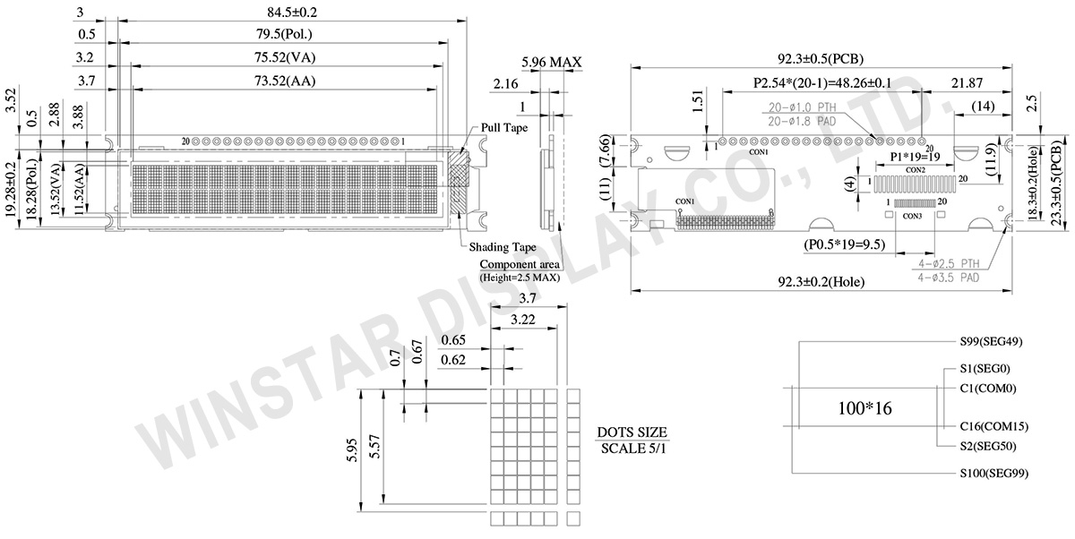
Données mécaniques
| Article | Dimensions | Unité |
|---|---|---|
| Format d'affichage | 2 lignes de 20 caractères | - |
| Dimensions du module | 92.3 x 23.3 x 5.96 Max. | mm |
| Zone active | 73.52 x 11.52 | mm |
| Taille des points | 0.62 x 0.67 | mm |
| Pas des points | 0.65 x 0.70 | mm |
| Taille des caractères | 3.22 x 5.57 | mm |
| Character pitch | 3.70 x 5.95 | mm |
| LCD type | OLED , Monochrome | |
| Duty | 1/16 | |
| IC | SSD1311 | |
| Interface | 6800, 8080, SPI, I2C | |
| Diagonale | 2.93 pouces | |
Valeurs nominales maximales absolues
| Article | Symbole | Min | Max | Unité |
|---|---|---|---|---|
| Supply Voltage For Logic | VDD-VSS | -0.3 | 3.6 | V |
| Température de fonctionnement | TOP | -40 | +80 | °C |
| Température de stockage | TST | -40 | +85 | °C |
Caractéristiques électroniques
DC Caractéristiques électroniques
| Article | Symbole | État | Min | Typ | Max | Unité |
|---|---|---|---|---|---|---|
| Supply Voltage For Logic | VDD-VSS | - | 3.1 | 3.3 | 3.5 | V |
| Input High Volt. | VIH | - | 0.8xVDD | - | - | V |
| Input Low Volt. | VIL | - | - | - | 0.2xVDD | V |
| Output High Volt. | VOH | IOH=-0.5mA | 0.9xVDD | - | - | V |
| Output Low Volt. | VOL | IOL=0.5mA | - | - | 0.1xVDD | V |
| 50% Check Board Operating Current |
IDD | VDD=3.3V | - | 50 | 75 | mA |
Search keyword: oled 20x2, 20x2 oled
