


Modules Afficheurs OLED Graphiques COG 2.42"
N° de modèle WEO012864AJ
►Type: Graphique
►Structure: COG
►Dimension: 2.42 pouces
►Matrice de points 128 x 64
►IC:CH1116
►Alimentation 3V
►1/64 duty
►Interface: I2C,4-line SPI,8-bits 6800/8080 parallel
►Couleur d'affichage: Blanc / Jaune
►MOQ:150K. Vous pouvez choisir WEO012864AL en remplacement de WEO012864AJ.
Description
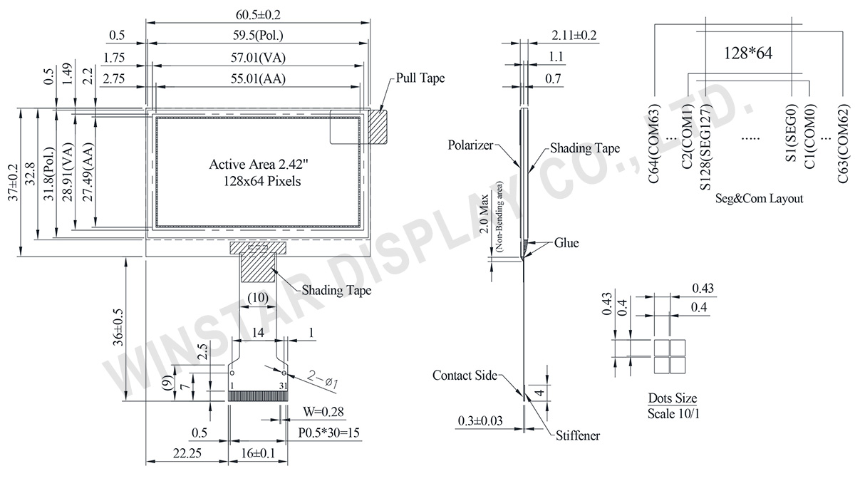
DESSIN
Data source ref:WEO012864AJWPP3N00000
SPÉCIFICATIONS
Fonction PIN sur l'interface
| No. | Symbole | Function | |||||||||||||||
|---|---|---|---|---|---|---|---|---|---|---|---|---|---|---|---|---|---|
| 1 | NC(GND) | No connection | |||||||||||||||
| 2 | VSS | Ground. | |||||||||||||||
| 3-10 | NC | No connection | |||||||||||||||
| 11 | VDD1 | Power supply input | |||||||||||||||
| 12 | IM1 | These are the MPU interface mode select pads.
(1) 0 is connected to VSS (2) 1 is connected to VDD1 |
|||||||||||||||
| 13 | IM2 | ||||||||||||||||
| 14 | NC | No connection | |||||||||||||||
| 15 | CS# | This pad is the chip select input. When CS# = “L”, then the chip select becomes active, and data/command I/O is enabled. | |||||||||||||||
| 16 | RES# | This is a reset signal input pad. When RES# is set to “L”, the settings are initialized. The reset operation is performed by the RES# signal level. | |||||||||||||||
| 17 | A0 | This is the Data/Command control pad that determines whether the data bits are data or a command. A0 = “H”: the inputs at D0 to D7 are treated as display data. A0 = “L”: the inputs at D0 to D7 are transferred to the command registers. In I2C interface, this pad serves as SA0 to distinguish the different address of OLED driver. |
|||||||||||||||
| 18 | WR# (R/W#) |
This is a MPU interface input pad. When connected to an 8080 MPU, this is active LOW. This pad connects to the 8080 MPU WR# signal. The signals on the data bus are latched at the rising edge of the WR# signal. When connected to a 6800 Series MPU: This is the read/write control signal input terminal. When R/W#= “H”: Read. When R/W#= “L”: Write. |
|||||||||||||||
| 19 | E/RD# | This is a MPU interface input pad. When connected to an 8080 series MPU, it is active LOW. This pad is connected to the RD# signal of the 8080 series MPU, and the data bus is in an output status when this signal is “L”. When connected to a 6800 series MPU, this is active HIGH. This is used as an enable clock input of the 6800 series MPU. When RD# = “H”: Enable. When RD# = “L”: Disable. |
|||||||||||||||
| 20~27 | D0~D7 | This is an 8-bit bi-directional data bus that connects to an 8-bit or 16-bit standard MPU data bus. When the serial interface is selected, then D0 serves as the serial clock input pad (SCL) and D1 serves as the serial data input pad (SI). At this time, D2 to D7 are set to high impedance. When the I2C interface is selected, then D0 serves as the serial clock input pad (SCL) and D1 serves as the serial data input pad (SDAI). At this time, D2 to D7 are set to high impedance. |
|||||||||||||||
| 28 | IREF | This is a segment current reference pad. A resistor should be connected between this pad and VSS. Set the current at 18.75uA. | |||||||||||||||
| 29 | VCOMH | This is a pad for the voltage output high level for common signals. A capacitor should be connected between this pad and VSS. |
|||||||||||||||
| 30 | VPP | OLED panel power supply. Generated by internal charge pump. Connect to capacitor. It could be supplied externally. |
|||||||||||||||
| 31 | NC(GND) | No connection |
Données mécaniques
| Article | Dimensions | Unité |
|---|---|---|
| Matrice de points | 128 x 64 | dots |
| Dimensions du module | 60.5 × 37.0 × 2.11 | mm |
| Zone active | 55.01 × 27.49 | mm |
| Pixel Size | 0.40 × 0.40 | mm |
| Pixel Pitch | 0.43 × 0.43 | mm |
| Mode d'affichage | Matrice passive | |
| Couleur d'affichage | Monochrome | |
| Drive Duty | 1/64 Duty | |
| IC | CH1116 | |
| Interface | I2C,4-line SPI,8-bits 6800/8080 parallel | |
| Diagonale | 2.42 pouces | |
Valeurs nominales maximales absolues
| Parameter | Symbole | Min | Max | Unité |
|---|---|---|---|---|
| Supply Voltage for Logic | VDD | -0.3 | 3.6 | V |
| Supply Voltage for Display | VCC | 0 | 14.5 | V |
| Température de fonctionnement | TOP | -40 | +80 | °C |
| Température de stockage | TSTG | -40 | +85 | °C |
Caractéristiques électroniques
| Article | Symbole | État | Min | Typ | Max | Unité |
|---|---|---|---|---|---|---|
| Supply Voltage for Logic | VDD1 | - | 1.65 | 3.0 | 3.3 | V |
| Supply Voltage for Display | VPP | - | 6.4 | 13.0 | 13.5 | V |
| High Level Input | VIH | - | 0.8×VDD1 | - | VDD1 | V |
| Low Level Input | VIL | - | VSS | - | 0.2×VDD1 | V |
| High Level Output | VOH | - | 0.8×VDD1 | - | VDD1 | V |
| Low Level Output | VOL | - | VSS | - | 0.2×VDD1 | V |
| Display 50% Pixel on | IPP | VPP =13V | - | 15 | 30 | mA |
Search keyword: 128x64 oled, oled 128x64, 2.42 oled, 2.42" oled, 2.42 inch oled, oled 2.42, oled 2.42"
