


N° de modèle WEO009664A
►Type: Graphique
►Structure: COG
►Dimension: 0.95 pouces
►Matrice de points 96 x 64
►IC:SSD1305
►Alimentation 3V
►1/64 duty
►Interface: 6800, 8080, SPI, I2C
►Couleur d'affichage: Blanc / Jaune
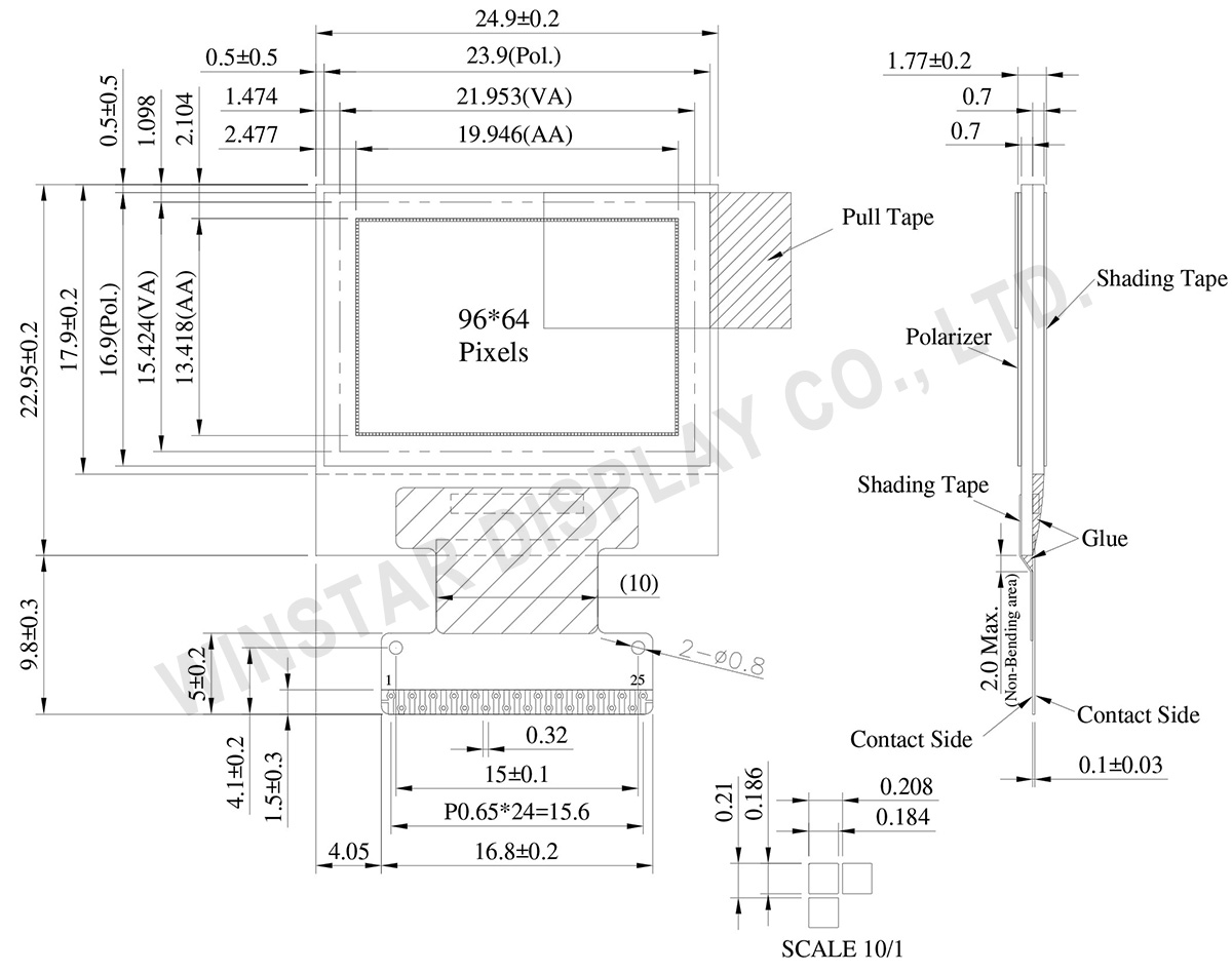
DESSIN
Data source ref: WEO009664ALPP3N00000
SPÉCIFICATIONS
Fonction PIN sur
| Pin Number | Symbole | I/O | Description | |||||||||||||||
|---|---|---|---|---|---|---|---|---|---|---|---|---|---|---|---|---|---|---|
| 1. | N.C. (GND) | - | Reserved Pin(Supporting Pin) The supporting pins can reduce the influences from stresses on the function pins. These pins must be connected to external ground. |
|||||||||||||||
| 2. | VCC | P | Power Supply for OLED Panel This is the most positive voltage supply pin of the chip.It must be supplied externally. |
|||||||||||||||
| 3. | VSS | P | Ground of Logic Circuit This is a ground pin. It also acts as a reference for the logic pins. It must be connected to external ground. |
|||||||||||||||
| 4. | VDD | P | Power Supply for Logic Circuit This is a voltage supply pin. It must be connected to external source. |
|||||||||||||||
| 5. | VDDIO | P | Power supply for interface logic level. It should be match with MCU interface voltage level. VDDIO must always be equal or lower than VDD. |
|||||||||||||||
| 6. | BS1 BS2 |
I | Communicating Protocol Select These pins are MCU interface selection input. See the following table:
|
|||||||||||||||
| 7. | ||||||||||||||||||
| 8. | CS# | I | Chip Select This pin is the chip select input. The chip is enabled for MCU communication only when CS# is pulled low. |
|||||||||||||||
| 9. | RES# | I | Power Reset for Controller and Driver This pin is reset signal input. When the pin is low, initialization of the chip is executed. |
|||||||||||||||
| 10. | D/C# | I | Data/ Command Control This pin is Data/Command control pin. When the pin is pulled high, the input at D7~D0 is treated as display data. When the pin is pulled low, the input at D7~D0 will be transferred to the command register. For detail relationship to MCU interface signals, please refer to the Timing Characteristics Diagrams. When the pin is pulled high and serial interface mode is selected, the data at SDIN is treated as data. When it is pulled low, the data at SDIN will be transferred to the command register. In I2C mode, this pin acts as SA0 for slave address selection. |
|||||||||||||||
| 11. | R/W# | I | Read/ Write Selector Write This pin is MCU interface input. When interfacing to a68XX-series microprocessor, this pin will be used as Read/Write (R/W#) selection input. Pull this pin to “High” for read mode and pull it to “Low” for write mode. When 80XXinterface mode is selected, this pin will be the Write (WR#) input. Data write operation is initiated when this pin is pulled low and the CS# is pulled low. |
|||||||||||||||
| 12. | E/RD# | I | Read/Write Enable or Read This pin is MCU interface input. When interfacing to a68XX-series microprocessor, this pin will be used as the Enable (E) signal. Read/write operation is initiated when this pin is pulled high and the CS# is pulled low. When connecting to an 80XX-microprocessor, this pin receives the Read (RD#) signal. Data read operation is initiated when this pin is pulled low and CS# is pulled low. |
|||||||||||||||
| 13. | D0~D7 | I/O | Host Data In put/ Output Bus These pins are 8-bit bi-directional data bus to be connected to the microprocessor’s data bus. When serial mode is selected, D1 will be the serial data input SDIN and D0 will be the serial clock input SCLK. When I2Cmode is selected, D2 & D1 should be tired together and serve as SDAout & SDAin in application and D0 is the serial clock input SCL. |
|||||||||||||||
| 14. | ||||||||||||||||||
| 15. | ||||||||||||||||||
| 16. | ||||||||||||||||||
| 17. | ||||||||||||||||||
| 18. | ||||||||||||||||||
| 19. | ||||||||||||||||||
| 20. | ||||||||||||||||||
| 21. | IREF | I | Current Reference for Brightness Adjustment This pin is segment current reference pin. A resistor should be connected between this pin and VSS. Set the current lower than 10μA. |
|||||||||||||||
| 22. | VCOMH | O | Voltage Output High Level for COM Signal This pin is the input pin for the voltage output high level for COM signals. A capacitor should be connected between this pin and VSS. |
|||||||||||||||
| 23. | VCC | P | Power Supply for OLED Panel This is the most positive voltage supply pin of the chip.It must be supplied externally. |
|||||||||||||||
| 24. | VLSS | P | Ground of Analog Circuit This is an analog ground pin. It should be connected to VSS externally. |
|||||||||||||||
| 25. | N.C. (GND) | - | Reserved Pin(Supporting Pin) The supporting pins can reduce the influences from stresses on the function pins. These pins must be connected to external ground. |
Données mécaniques
| Article | Dimensions | Unité |
|---|---|---|
| Matrice de points | 96 x 64 Dots | - |
| Dimensions du module | 24.9 × 22.95 × 1.77 | mm |
| Zone active | 19.946 × 13.418 | mm |
| Taille des points | 0.184 × 0.186 | mm |
| Pas des points | 0.208 × 0.21 | mm |
| Mode d'affichage | Matrice passive | |
| Couleur d'affichage | Monochrome | |
| Drive Duty | 1/64 Duty | |
| IC | SSD1305 | |
| Interface | 6800,8080,4-Wire SPI,I2C | |
| Diagonale | 0.95 pouces | |
Valeurs nominales maximales absolues
| Parameter | Symbol | Min | Max | Unité |
|---|---|---|---|---|
| Supply Voltage for Logic | VDD | -0.3 | 4 | V |
| Supply Voltage for Display | VCC | 0 | 15 | V |
|
Logic Supply Voltage for MCU interface |
VDDIO | 0.3 | VDD+0.5 | V |
| Température de fonctionnement | TOP | -40 | +80 | °C |
| Température de stockage | TSTG | -40 | +85 | °C |
Caractéristiques électroniques
DC Caractéristiques électroniques
| Article | Symbol | État | Min | Typ | Max | Unité |
|---|---|---|---|---|---|---|
| Supply Voltage for Logic | VDD | - | 2.8 | 3.0 | 3.3 | V |
| Supply Voltage for Display | VCC | - | 11.5 | 12 | 12.5 | V |
| Logic Supply Voltage for MCU interface | VDDIO | - | 1.6 | - | VDD | V |
| Input High Volt. | VIH | - | 0.8×VDDIO | - | VDDIO | V |
| Input Low Volt. | VIL | - | 0 | - | 0.2×VDDIO | V |
| Output High Volt. | VOH | - | 0.9×VDDIO | - | VDDIO | V |
| Output Low Volt. | VOL | - | 0 | - | 0.1×VDDIO | V |
| 50% Check Board operating Current | ICC | VCC=12V | - | 6.0 | 7.5 | mA |
Search keyword: 96x64 oled, oled 96x64, 0.95 oled, 0.95" oled, 0.95 pouces oled, oled 0.95"
