


Afficheur Portables 0.91 pouces, 128x32
N° de modèle WEO012832D
►2017 Taiwan Excellence Award
►Type: Graphique (sans cadre)
►Structure: COG
►Dimension: 0.91 pouces
►Suitable for wearable device
►Matrice de points 128 x 32
►IC:SSD1306
►Alimentation 3V
►1/32 duty
►Interface: SPI
►Couleur d'affichage: Blanc / Jaune / Bleu ciel
►Autres options FPC disponibles dans le tableau ci-dessous
Description

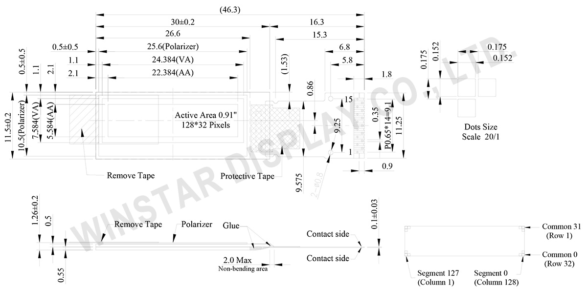
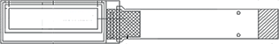
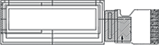
DESSIN
Data source ref: WEO012832DWPP3N00008
SPÉCIFICATIONS
Fonction PIN sur l'interface
| No. | Symbole | Fonction |
|---|---|---|
| 1 | C2P | Positive Terminal of the Flying Inverting Capacitor Negative Terminal of the Flying Boost CapacitorThe charge-pump capacitors are required between the terminals. They must be floated when the converter is not used. |
| 2 | C2N | |
| 3 | C1P | |
| 4 | C1N | |
| 5 | VBAT | Power Supply for DC/DC Converter Circuit This is the power supply pin for the internal buffer of the DC/DC voltage converter. It must be connected to external source when the converter is used. It should be connected to VDD when the converter is not used. |
| 6 | VSS | Ground of Logic Circuit This is a ground pin. It acts as a reference for the logic pins. It must be connected to external ground. |
| 7 | VDD | Power Supply for Logic This is a voltage supply pin. It must be connected to external source. |
| 8 | CS# | Chip Select This pin is the chip select input. The chip is enabled for MCU communication only when CS# is pulled low. |
| 9 | RES# | Power Reset for Controller and Driver This pin is reset signal input. When the pin is low, initialization of the chip is executed. |
| 10 | D/C# | Data/Command Control This pin is Data/Command control pin.. When the pin is pulled high and serial interface mode is selected, the data at SDIN is treated as data. When it is pulled low, the data at SDIN will be transferred to the command register. |
| 11 | SCLK | When serial mode is selected, D1 will be the serial data input SDIN and D0 will be the serial clock input SCLK. |
| 12 | SDIN | |
| 13 | IREF | Current Reference for Brightness Adjustment This pin is segment current reference pin. A resistor should be connected between this pin and VSS. Set the current lower than 30uA. |
| 14 | VCOMH | Voltage Output High Level for COM Signal This pin is the input pin for the voltage output high level for COM signals. A capacitor should be connected between this pin and VSS. |
| 15 | VCC | Power Supply for OEL Panel This is the most positive voltage supply pin of the chip. A stabilization capacitor should be connected between this pin and VSS when the converter is used. It must be connected to external source when the converter is not used. |
Spécifications générales
| Article | Dimensions | Unité |
|---|---|---|
| Matrice de points (Résolution) | 128 × 32 | points |
| Dimensions du module | 30.0 × 11.5 × 1.26 | mm |
| Zone active | 22.384 × 5.584 | mm |
| Taille des points | 0.152 × 0.152 | mm |
| Pas des points | 0.175 × 0.175 | mm |
| Mode d'affichage | Matrice passive | |
| Couleur d'affichage | Monochrome | |
| Drive Duty | 1/32 Duty | |
| IC | SSD1306 | |
| Interface | 4-wire SPI | |
| Diagonale | 0.91 pouces | |
Valeurs nominales maximales absolues
| Parameter | Symbole | Valeur min | Valeur max | Unité |
|---|---|---|---|---|
| Supply Voltage for Logic | VDD | 0 | 4.0 | V |
| Supply Voltage for Display | VCC | 0 | 16.0 | V |
| Température de fonctionnement | TOP | -40 | +80 | °C |
| Température de stockage | TSTG | -40 | +85 | °C |
Caractéristiques électroniques
DC Caractéristiques électroniques
| Article | Symbole | État | Valeur min | Valeur type | Valeur max | Unité |
|---|---|---|---|---|---|---|
| Supply Voltage for Logic | VDD | - | 2.8 | 3.0 | 3.3 | V |
| Supply Voltage for Display (Supplied Externally) | VCC | - | 7 | 7.25 | 8 | V |
| Charge Pump Regulator Supply Voltage | VBAT | - | 3.0 | - | 4.2 | V |
| Charge Pump Output Voltage for Display (Generated by Internal DC/DC) | Charge Pump VCC |
- | 7.0 | 7.5 | - | V |
| Input High Volt. | VIH | - | 0.8×VDD | - | VDD | V |
| Input Low Volt. | VIL | - | 0 | - | 0.2×VDD | V |
| Output High Volt. | VOH | - | 0.9×VDD | - | VDD | V |
| Output Low Volt. | VOL | - | 0 | - | 0.1×VDD | V |
| Operating Current for VCC (VCC Supplied Externally) | ICC | VCC =7.25V | - | 7 | 11 | mA |
| Display 50% Pixel on (VCC Generated by Internal DC/DC) | IBAT | - | - | 15 | 25 | mA |
Options de FPC:
| Image | FPC Length | PIN | pitch | ZIF FPC or HOTBAR FPC | Interface | FPC No. | Create Date |
|---|---|---|---|---|---|---|---|
 |
17.06 | 15 | 0.65 | HOTBAR FPC | SPI | FPC2065001501XXXXX00 | 20140827 |
 |
40.76 | 15 | 0.5 | ZIF FPC | SPI | FPC2050001511XXXXX02 | 20150421 |
 |
11.26 | 14 | 0.62 | HOTBAR FPC | I2C | FPC2062001401XXXXX02 | 20160106 |
Search keyword: 128x32 oled, oled 128x32, 0.91 oled, 0.91" oled, 0.91 pouces oled, oled 0.91, oled 0.91"
