


Pantalla TFT Táctil Capacitivo 5.7 pulgada
Modelo Nº WF57VTIACDNG0
►Tamaño : 5.7 pulgada
►Resolución : 320 x 240 puntos
►Dirección de la vista : 12H
►Interfaz : RGB
►Driver IC:HX8218+HX8615
►Placa de control : No
►Brillo (cd/m²): 400
►Agujero del bastidor : Yes
►Pantalla táctil : Con panel táctil capacitivo (PCAP)
►Detect Point : 5 Fingers
►O-Film : Opcional
Descripción
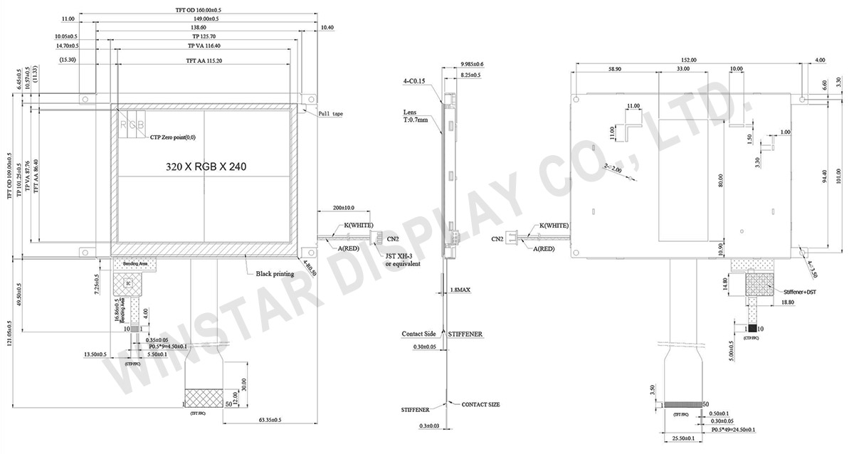
El WF57VTIACDNG0 es un TFT LCD estándar de 5.7 pulgadas que presume una resolución de 320 x 240 puntos y una luminosidad de 400 cd/m². Equipado con un circuito integrado de controladores HX8218+HX8615 que soporta interfaces RGB de 24 bits, este módulo TFT opera con una alimentación de voltaje de 3.3V (valor típico). Sus dimensiones de módulo miden 160 mm de ancho y 109 mm de alto, con un área activa de 115.20 mm x 86.40 mm.
El WF57VTIACDNG0 presenta una dirección de visualización a las 12 en punto, una inversión de grises a las 6 en punto y una relación de aspecto de 4:3. Con un rango de temperatura de operación desde -20°C hasta +70°C y un rango de temperatura de almacenamiento que abarca desde -30°C hasta +80°C, garantiza fiabilidad en diversos entornos.
Este modelo está equipado con una pantalla táctil capacitiva proyectada, que integra el circuito integrado ILI2130 que soporta la interfaz I2C y ofrece funcionalidad de 5 puntos táctiles. Esta mejora hace que el WF57VTIACDNG0 sea ideal para aplicaciones que demandan interacción intuitiva del usuario, como dispositivos médicos, incluidos sistemas de monitoreo de pacientes, máquinas de ultrasonido y equipos de imágenes médicas. Además, resulta invaluable en sistemas de automatización y control industrial, proporcionando a los operadores datos en tiempo real y capacidades de control mejoradas para un funcionamiento y mantenimiento eficientes de las instalaciones industriales.
DIBUJO
ESPECIFICACIONES
Función interfaz Pin
LCM PIN Definition
| Pin | Símbolo | Función |
|---|---|---|
| 1 | IF1 | Input data format control |
| 2 | IF2 | Input data format control |
| 3 | POL | Polarity Signal connect to VCOM driving circuit. |
| 4 | RESET | Hardware reset |
| 5 | SPENA | Chip select |
| 6 | SPCL | Serial Clock |
| 7 | SPDA | Serial Data |
| 8 | B0 | Blue Data bit |
| 9 | B1 | Blue Data bit |
| 10 | B2 | Blue Data bit |
| 11 | B3 | Blue Data bit |
| 12 | B4 | Blue Data bit |
| 13 | B5 | Blue Data bit |
| 14 | B6 | Blue Data bit |
| 15 | B7 | Blue Data bit |
| 16 | G0 | Green Data bit |
| 17 | G1 | Green Data bit |
| 18 | G2 | Green Data bit |
| 19 | G3 | Green Data bit |
| 20 | G4 | Green Data bit |
| 21 | G5 | Green Data bit |
| 22 | G6 | Green Data bit |
| 23 | G7 | Green Data bit |
| 24 | R0 | Red Data bit |
| 25 | R1 | Red Data bit |
| 26 | R2 | Red Data bit |
| 27 | R3 | Red Data bit |
| 28 | R4 | Red Data bit |
| 29 | R5 | Red Data bit |
| 30 | R6 | Red Data bit |
| 31 | R7 | Red Data bit |
| 32 | Hsync | Horizontal synchronous signal |
| 33 | Vsync | Vertical synchronous signal |
| 34 | Data CLK | Dot data clock |
| 35 | AVDD(analog) | Analog power: 4.5V~5.5V |
| 36 | AVDD(analog) | Analog power: 4.5V~5.5V |
| 37 | VCC(Digital) | Digital power: 3V~3.6V |
| 38 | VCC(Digital) | Digital power: 3V~3.6V |
| 39 | NPC | NTSC/PAL mode Auto detection result H:NTSC/L:PAL |
| 40 | VGL | Gate off power |
| 41 | VGL | Gate off power |
| 42 | UD | Up/down selection |
| 43 | VGH | Gate on power |
| 44 | LRC | Shift direction of device internal shift register control. |
| 45 | GND | System ground pin of the IC. Connect to system ground. |
| 46 | VCOM | VCOM driving input |
| 47 | VCOM | VCOM driving input |
| 48 | ENB | Signal to settle the horizontal display position |
| 49 | GND | System ground pin of the IC. Connect to system ground. |
| 50 | GND | System ground pin of the IC. Connect to system ground. |
PCAP PIN Definition
| Pin | Símbolo | Función |
|---|---|---|
| 1 | VSS | System ground pin of the IC. Connect to system ground. |
| 2 | VDDT | Power Supply : +3.0V |
| 3 | SCL | I2C clock input |
| 4 | NC | No connect |
| 5 | SDA | I2C data input and output |
| 6 | NC | No connect |
| 7 | /RST | External Reset, Low is active |
| 8 | NC | No connect |
| 9 | /INT | External interrupt to the host |
| 10 | VSS | System ground pin of the IC. Connect to system ground. |
Especificaciones generales
| Elemento | Dimensión | Unidad |
|---|---|---|
| Tamaño | 5.7 | pulgada |
| Matriz de puntos | 320 × RGB × 240 (TFT) | dots |
| Dimensión del módulo | 160(W) × 109(H) × 9.985 (D) | mm |
| zona activa | 115.2 × 86.40 | mm |
| Distancia entre puntos | 0.12 × 0.36 | mm |
| Tipo de LCD | TFT, Blanco, Transmisivo | |
| Dirección de la vista | 12 o'clock | |
| Dirección de inversión de escala de grises | 6 o'clock | |
| TFT Interfaz | 24-bit RGB | |
| TFT Controlador IC | HX8218+HX8615o equivalente | |
| Relación de aspecto | 4:3 | |
| Tipo de retroiluminación | LED, Blanco | |
| PCAP FW Version | 0x07.0x00.0x00.0x00.0xA2.0x01.0x57.0x00 | |
| PCAP IC | ILI2130 o equivalente | |
| PCAP Interfaz | I2C | |
| PCAP Resolución | 16384*16384 | |
| Con o sin panel táctil | Con panel táctil capacitivo (PCAP) | |
| Superficie | Deslumbramiento | |
Valores nominales máximos absolutos
| Elemento | Símbolo | Valor mín. | Valor típico | Valor máx. | Unidad |
|---|---|---|---|---|---|
| Temperatura de funcionamiento | TOP | -20 | - | +70 | ℃ |
| Temperatura de almacenamiento | TST | -30 | - | +80 | ℃ |
Características electrónicas
| Elemento | Símbolo | Valor mín. | Valor típico | Valor máx. | Unidad |
|---|---|---|---|---|---|
| Supply Voltage For LCM | VCC | 3.2 | 3.3 | 3.4 | V |
| Supply Current For LCM | ICC | - | 30 | 45 | mA |
| Supply PCAP | VDDT | 3.1 | 3.3 | 3.5 | V |
| ICTP | - | 56 | 84 | mA | |
| Input High Volt. | VIH | 0.7 VCC | - | VCC | V |
| Input Low Volt. | VIL | 0 | - | 0.3 VCC | V |
| LCD Driving Supply Voltage |
VGH | 15 | 16 | 17 | V |
| VGL | -6 | -5 | -4 | V | |
| VCOMH | - | 4.5 | - | V | |
| VCOML | - | -0.5 | - | V | |
| AVDD | 4.5 | 5.0 | 5.5 | V |
