


2 Zoll 240x320 PCAP TFT IPS Bildschirm
Modellnummer WF0200BTYAJDNG10
►Größe: 2 Zoll
►Auflösung: 240 x 320 Punkten
►Betrachtungsrichtung: IPS
►Schnittstelle: MCU, SPI
►Treiber IC:ST7789VI
►Steuerplatine: Nein
►Helligkeit (cd/m²):400
►Durchsteckrahmen: Nein
►Touchscreen: Projiziert Kapazitiver Touchscreen (PCAP),OCA
►Berührungspunkte: 1 Finger
Beschreibung
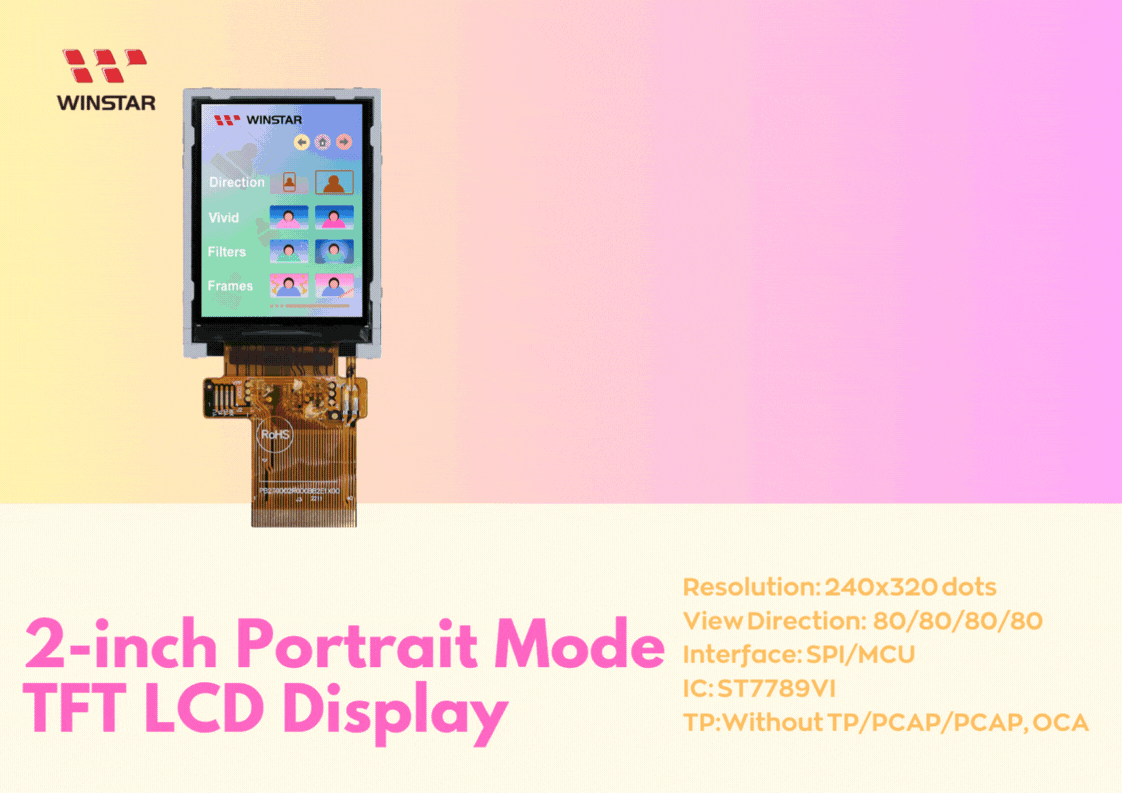
WF0200BTYAJDNG10 ist ein 2-Zoll High-Brightness IPS TFT-LCD-Modul im Porträtmodus mit einer Auflösung von 240x320 Pixeln. Es verwendet den ST7789VI Treiber-IC und unterstützt MCU- und SPI-Schnittstellen. Der PCAP-Touchscreen verfügt über den integrierten IC GT911 und unterstützt die I2C-Schnittstelle. Darüber hinaus verwendet das PCAP-Panel die OCA-Technologie, um die Haltbarkeit zu erhöhen und eine bessere optische Klarheit zu bieten.
WF0200BTYAJDNG10 hat einen weiten Betrachtungswinkel von Links: 80 / Rechts: 80 / Oben: 80 / Unten: 80 Grad, ein Kontrastverhältnis von 800:1, eine Helligkeit von 400 Nits und ein Seitenverhältnis von 3:4. Die Versorgungsspannung für analoge Signale beträgt 2,4V bis 3,6V (typischer Wert: 3,3V). Dieses TFT-LCD-Modul kann in einem Temperaturbereich von -20℃ bis +70℃ betrieben werden, und die Lagertemperaturen liegen zwischen -30℃ und +80℃.
Der 2-Zoll-TFT-LCD-Display im Hochformat eignet sich für eine Vielzahl von elektronischen Geräten, darunter Messgeräte wie Laserentfernungsmesser und Luftqualitätsdetektoren, sowie Testgeräte, Sportuhren und andere kompakte elektronische Geräte. Unsere WF0200B TFT-Serie bietet die Option ohne Touchpanel; bitte besuchen Sie die Webseite des Modells WF0200BSYAJDNN0 für weitere Informationen.
Zeichnung
Technische Daten
Schnittstelle
LCM PIN Definition
| NO | Symbol | Funktion | |||||||||||||||||||||||||||||||||||
|---|---|---|---|---|---|---|---|---|---|---|---|---|---|---|---|---|---|---|---|---|---|---|---|---|---|---|---|---|---|---|---|---|---|---|---|---|---|
| 1 | GND | Ground | |||||||||||||||||||||||||||||||||||
| 2 | NC(YU) | No connection | |||||||||||||||||||||||||||||||||||
| 3 | NC(XL) | No connection | |||||||||||||||||||||||||||||||||||
| 4 | NC(YD) | No connection | |||||||||||||||||||||||||||||||||||
| 5 | NC(XR) | No connection | |||||||||||||||||||||||||||||||||||
| 6 | NC | No connection | |||||||||||||||||||||||||||||||||||
| 7 | VDD | Power supply | |||||||||||||||||||||||||||||||||||
| 8 | VDDI | Power Supply for I/O System. | |||||||||||||||||||||||||||||||||||
| 9 | TE | Tearing effect signal is used to synchronize MCU to frame memory writing. If not used, please let this pin open |
|||||||||||||||||||||||||||||||||||
| 10 | CSX | Chip selection pin Low enable. High disable. |
|||||||||||||||||||||||||||||||||||
| 11 | DCX(SCL) | (D/CX): This pin is used to select “Data or Command” in the parallel interface. DCX=’1’: display data or parameter. DCX=’0’: command data. (SCL): When SPI mode,This pin is used to be serial interface clock. |
|||||||||||||||||||||||||||||||||||
| 12 | WRX(D/CX) | Display data/command selection Second Data lane in 2 data lane serial interface. (WRX): Write enable in MCU parallel interface. (D/CX): When 4-SPI mode,This pin in 4-line serial interface If not used, please fix this pin at VDDI or GND. |
|||||||||||||||||||||||||||||||||||
| 13 | RDX | -Read enable in 8080 MCU parallel interface. -If not used, please fix this pin at VDDI or GND. |
|||||||||||||||||||||||||||||||||||
| 14~29 | DB0~DB15 | Data bus line | |||||||||||||||||||||||||||||||||||
| 30 | RESX | System reset pin. signal is active low |
|||||||||||||||||||||||||||||||||||
| 31 | IM0 | The MCU interface mode select.
|
|||||||||||||||||||||||||||||||||||
| 32 | IM1 | ||||||||||||||||||||||||||||||||||||
| 33 | IM2 | ||||||||||||||||||||||||||||||||||||
| 34~35 | DB16~DB17 | Data bus line | |||||||||||||||||||||||||||||||||||
| 36 | VLED- | Cathode of LED backlight. | |||||||||||||||||||||||||||||||||||
| 37 | VLED- | Cathode of LED backlight. | |||||||||||||||||||||||||||||||||||
| 38 | VLED+ | Anode of LED backlight. | |||||||||||||||||||||||||||||||||||
| 39 | NC(SDA) | When SPI mode, This pin is SPI interface input/output pin. The data is latched on the rising edge of the SCL signal. If not used(NC), please fix this pin at VDDI or GND level. |
|||||||||||||||||||||||||||||||||||
| 40 | NC | No connection |
PCAP PIN Definition
| Pin | Symbol | Funktion |
|---|---|---|
| 1 | VSS | Ground for analog circuit |
| 2 | VDDT | Power Supply : |
| 3 | SCL | I2C clock inputI2C clock input |
| 4 | NC | No connect |
| 5 | SDA | I2C data input and output |
| 6 | NC | No connect |
| 7 | /RST | External Reset, Low is active |
| 8 | NC | No connect |
| 9 | /INT | External interrupt to the host |
| 10 | VSS | Ground for analog circuit |
Allgemeine Spezifikationen
| Artikel | Ausmaß | Einheit |
|---|---|---|
| Größe | 2 | Zoll |
| Punktmatrix | 240 x RGB x 320(TFT) | dots |
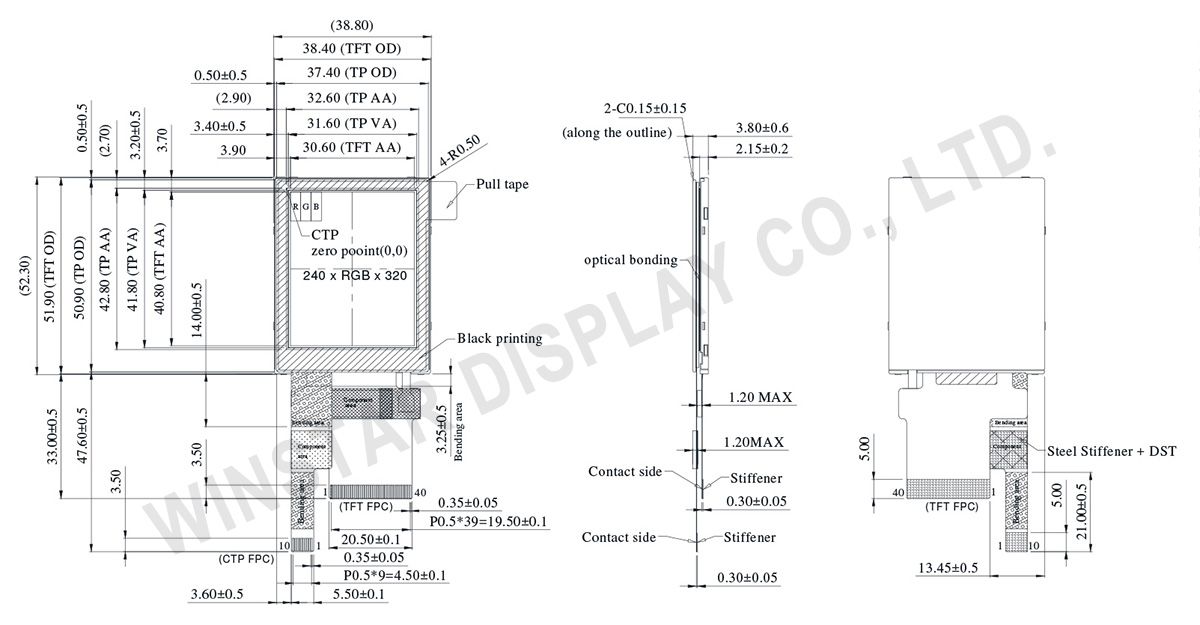
| Abmaße der modul | 38,8(W) x 52,3(H) x3,8(D) | mm |
| Aktiver Bereich | 30,60 x 40,80 | mm |
| Pixelabstand | 0.1275 x 0.1275 | mm |
| LCD-Typ | TFT, Schwarz, Transmissiv | |
| TFT Schnittstelle | MCU / SPI | |
| TFT Treiber IC | ST7789VI oder gleichwertig | |
| Betrachtungsrichtung | 80/80/80/80 (IPS) | |
| Seitenverhältnis | 3:4 | |
| Backlight-Typ | LED, Weiß | |
| PCAP Treiber IC | GT911 oder gleichwertig | |
| PCAP Schnittstelle | I2C | |
| FW Version | V92 | |
| PCAP Auflösung | 240 * 320 | |
| Touchscreen | Kapazitiv Touchscreen (PCAP) | |
| Oberfläche | Glanz | |
absolute Grenzwerte
| Artikel | Symbol | Mindestwert | typischer Wert | Maximalwert | Einheit |
|---|---|---|---|---|---|
| Betriebstemperatur | TOP | -20 | - | 70 | ℃ |
| Lagertemperatur | TST | -30 | - | 80 | ℃ |
elektrische Eigenschaften
| Artikel | Symbol | Condition | Mindestwert | typischer Wert | Maximalwert | Einheit |
|---|---|---|---|---|---|---|
| Supply Voltage For Analog | VDD | - | 2,4 | 3,3 | 3,6 | V |
| Interface Operation Voltage | VDDI | - | 1,65 | 1,8 | 3,6 | V |
| Supply Current For LCM | IDD | VDD = VDDI = VCC=3.0V |
- | 6,0 | 9,0 | mA |
| Supply PCAP | VPCAP | - | 2,8 | - | 3,3 | V |
| IPCAP | - | - | 8,0 | 12,0 | mA |
