
Issue No. 157
- Contents
- 1) WF43XTWAGDNG0 – 4.3 inch 800x480 IPS TFT with PCAP Touch
- 2) WF101KTYAPLNN0– 10.1 inch 1280x800 IPS TFT-LCD
- 3) WF101LSYAPLNN0 – 10.1 inch High Brightness 1280x800 IPS TFT
- 4) Getting to Know Display Interfaces
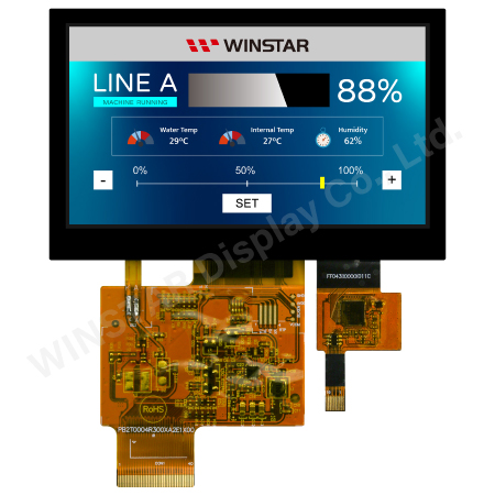
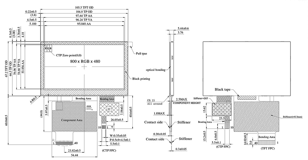
WF43XTWAGDNG0 – 4.3 inch 800x480 IPS TFT with PCAP Touch
WF43XTWAGDNG0 is a 4.3-inch Wide Temperature IPS TFT-LCD display with a Projected Capacitive Touch screen, made of resolution 800x480 pixels. This module is built-in with HX8264 and HX8664 driver ICs, and it supports 24-bit RGB interface. WF43XTWAGDNG0 is adopted IPS panel which is having the advantage of wider view angle of Left:80 / Right:80 / Up:80 / Down:80 degree (typical), contrast ratio 800:1 (typical value), brightness 500 nits (typical value), glare surface panel, aspect ratio 16:9. The PCAP touch screen is built-in with ILI2130 IC, supporting I2C interface and multi-touch function. The WF43X model has a projected capacitive touch panel (PCAP) and without a touch panel option (WF43XTWAGDNN0).
The supply voltage (VCC) of WF43XTWAGDNG0 is from 3.0V to 3.6V, the typical value of 3.3V. It can be operating at temperatures from -30℃ to+ 80℃ and storage temperatures from -30℃ to +80℃.
|
 |
► Link to WF43XTWAGDNG0 web page

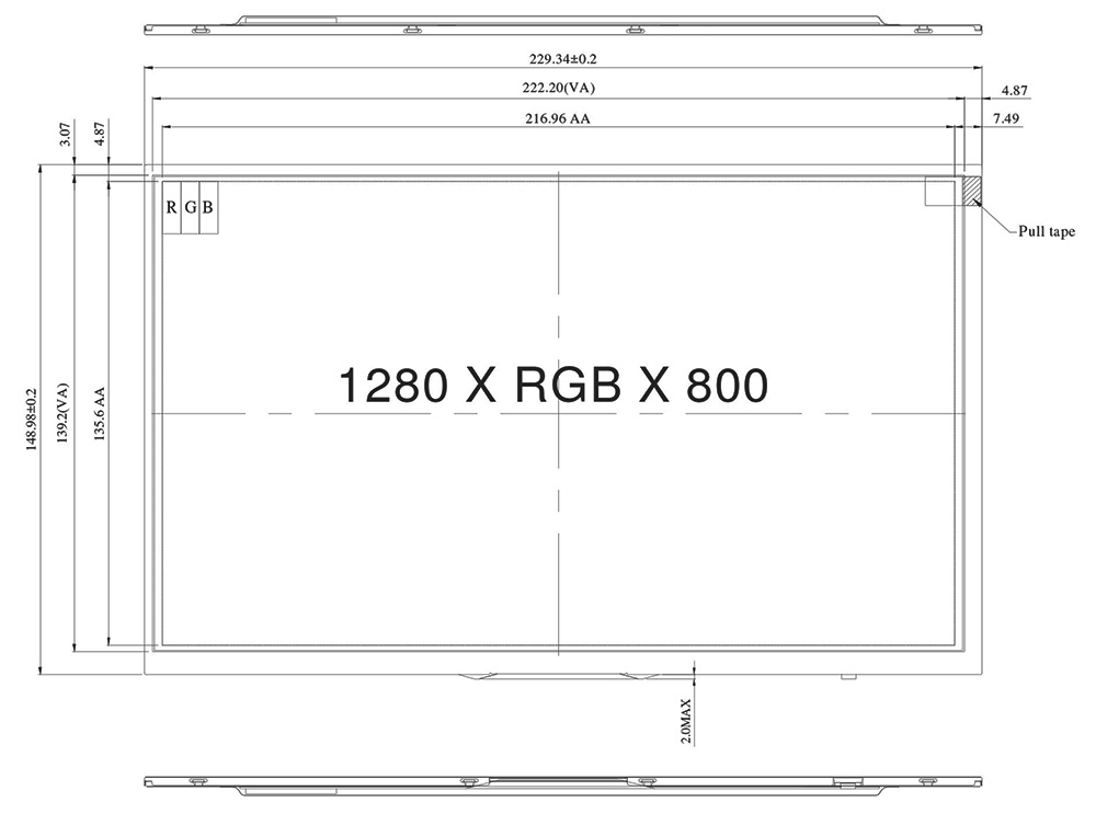
WF101KTYAPLNN0– 10.1 inch 1280x800 IPS TFT-LCD
WF101KTYAPLNN0 is a 10.1-inch IPS TFT-LCD display, made of resolution 1280x800 pixels. This module is built-in with EK79202B1 driver IC, and it supports LVDS interface. WF101KTYAPLNN0 is adopted IPS panel which is having the advantage of wider view angle of Left:80 / Right:80 / Up:80 / Down:80 degree (typical), contrast ratio 1000:1 (typical value), brightness 350 nits (minimum value), anti-glare surface panel, aspect ratio 16:10. WF101K model is also available in projected capacitive touch screen (PCAP) and resistive touch screen (RTP).
The supply voltage (VCC) of WF101KTYAPLNN0 is from 3.0V to 3.5V, the typical value of 3.3V. It can be operating at temperatures from -20℃ to+ 70℃ and storage temperatures from -30℃ to +80℃.
|
 |
► Link to WF101KTYAPLNN0 web page
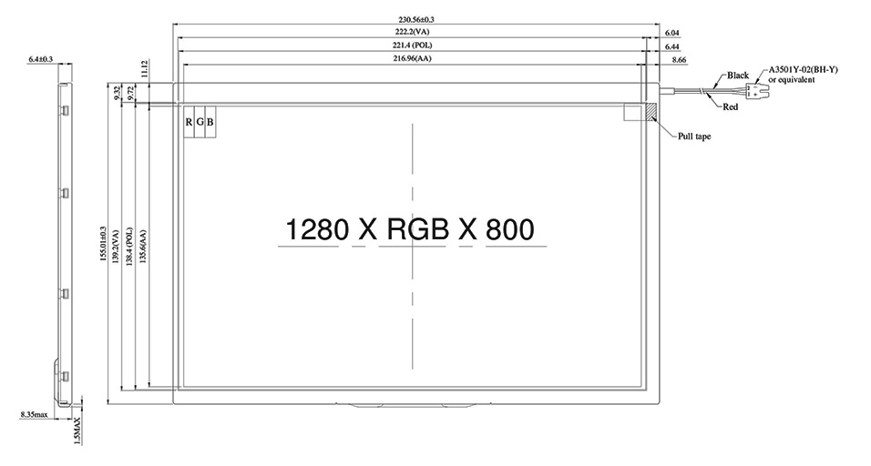
WF101LSYAPLNN0 – 10.1 inch High Brightness 1280x800 IPS TFT
WF101LSYAPLNN0 is a 10.1-inch High Brightness IPS TFT-LCD module, made of resolution 1280x800 pixels. This module is built-in with EK79202B1 driver IC, and it supports LVDS interface. WF101LSYAPLNN0 is adopted IPS panel which is having the advantage of wider view angle of Left:80 / Right:80 / Up:80 / Down:80 degree (typical), contrast ratio 1000:1 (typical value), brightness 1100 nits (typical value), anti-glare surface panel, aspect ratio 16:10. WF101L model is also available in projected capacitive touch screen (PCAP) and resistive touch screen (RTP)..
The supply voltage (VCC) of WF101LSYAPLNN0 is from 3.0V to 3.5V, the typical value of 3.3V. It can be operating at temperatures from -20℃ to+ 70℃ and storage temperatures from -30℃ to +80℃.
|
 |
► Link to WF101LSYAPLNN0 web page
Getting to Know Display Interfaces
Preface:
Winstar provides thousands of model display modules, including TN/STN LCD, OLED, and TFT. And there are many types of interfaces to deliver image data to the display module. Customers may question which one is the best or can meet the requirement. This article will discuss an issue regarding the data transfer of display interfaces.
A significant issue with the display interface is Communication bandwidth (BW). Why is BW a matter? BW represents the measure of data transfer in the communication channel. So the BW affects display response to screen data, which means the display's refresh rate. The display performance, in other words.
Introduction:
Well-known display interfaces nowadays:
1.Parallel
1.1 MCU interface 8080/6800
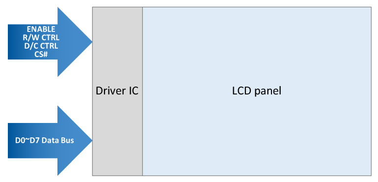
Display raw data sent via Data bus according to control bus signal. Communication bandwidth depends on enabling speed running on Driver IC. QVGA 320x240 dot matrix LCD i.e., the communication bandwidth will be 320 * 240 / 8 bit (data width) * 60 fps = 576KHz at ENABLE signal.
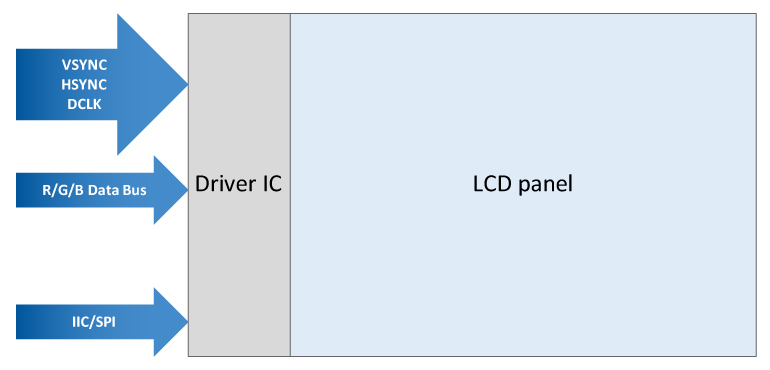
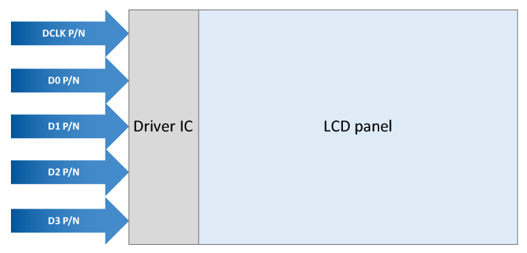
1.2 Parallel RGB 16/18/24 bits
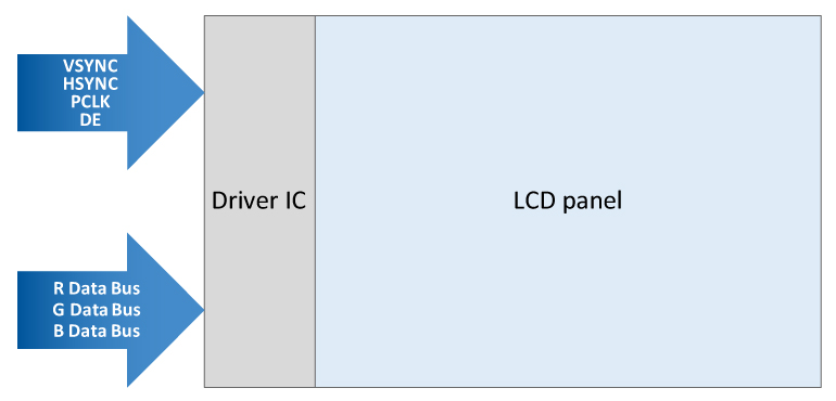
The RGB interface is to transmit the drive timing to the display driver IC through the data input/output in a parallel manner, including R/G/B data, vertical synchronization signal (V-SYNC, Vertical synchronizing signal), horizontal synchronization signal (H-SYNC), horizontal synchronizing signal), data enable (DE, Data Enable) signal, and clock signal PCLK (Pixel Clock). The display interface of RGB666 is as follows:
Display raw data transferred same as above. But the display resolution is getting higher and higher. i.e., WVGA 800 * 480 (pixels) * 60 fps = 23.04 MHz. (PCLK)
2.Serial
2.1 SPI (Serial Peripheral Interface)
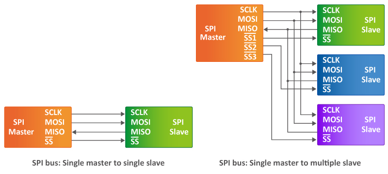
SPI is a master-slave-based interface, usually with a Master (master device) and one or multi slave (slave devices). There are 4 pins on the interface. The connection method and hardware structure are as follows:
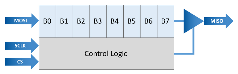
SCLK: The synchronous clock used by all devices. The master drives this clock and the slaves receive the clock.
MOSI: Master out, slave in. This is the main data line driven by the master to all slaves on the SPI bus. Only the selected slave clocks data from MOSI.
MISO: Master in, slave out. This is the main data line driven by the selected slave to the master. Only the selected slave may drive this circuit. In fact, it is the only circuit in the SPI bus arrangement that a slave is ever permitted to drive.
CS: Chip Select. This signal is unique to each slave. When active the selected slave must drive MISO.
Display data transferred in sequential. Display interface communication bandwidth i.e., QVGA 320 * 240 (pixels) * 16 bit (color depth) * 30 fps = 36.864 MHz.
2.2 IIC (Inter-Integrated Circuit) or alternatively known as I²C):
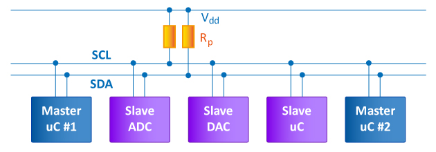
Different from the point-to-point (or point-to-multipoint) base of SPI, I²C is interfaced in the form of a data bus, which allows multiple master devices and multiple slave devices to be connected in series. The interface method and hardware structure are as follows:
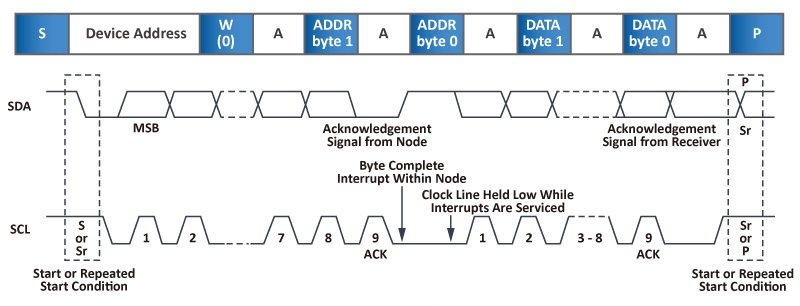
Standard mode = 100K bit/s.
Full speed mode = 400K bit/s.
Fast mode = 1M bit/s.
High speed mode = 3.2M bit/s.
2.3 Serial RGB 6/8 bits.
Display data transferred in RGB sequential. Display interface communication bandwidth i.e., QVGA 320 * 240 (pixels) * 3 dot * 30 fps = 6912000 Hz (DCLK).
2.4 LVDS: Low voltage differential signal. It should name FPD-Link for the display interface.
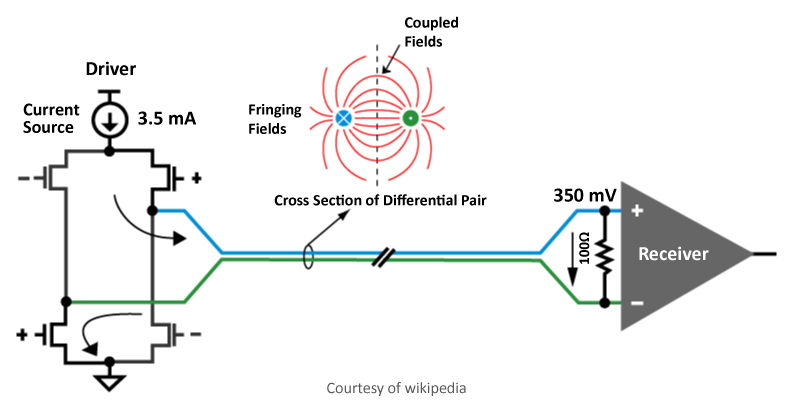
LVDS is a technical standard introduced in 1994 that specifies electrical characteristics of a differential, serial signaling standard, but it is not a protocol. LVDS is a physical layer specification only; many data communication standards and applications use it and add a data link layer as defined in the OSI model on top of it. LVDS operates at low power and can run at very high speeds using inexpensive twisted-pair copper cables.
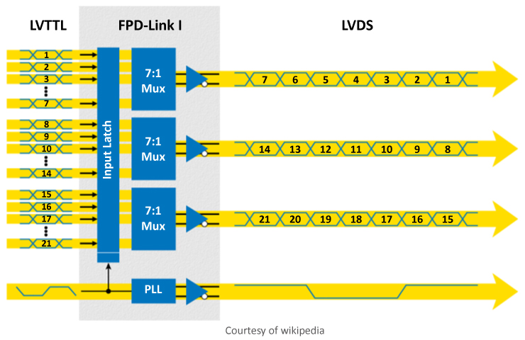
Early on, the notebook computer and LCD display vendors commonly used LVDS instead of FPD-Link when referring to their protocol. The term LVDS has mistakenly become synonymous with Flat Panel Display Link in the video-display engineering vocabulary.
2.5 MIPI CSI/DSI: Mobile Industry Processor Interface.
MIPI Alliance aimed at reducing the cost of display controllers in mobile devices. It defines a serial bus and a communication protocol between the host, the source of the image data, and the destination device. It is the expected target at LCD and similar display technologies.
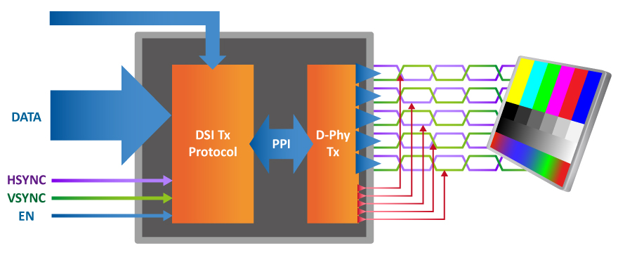
DSI specifies a high-speed (e.g., 4.5 Gbit/s/lane for D-PHY 2.0) differential signaling point-to-point serial bus. This bus includes one high-speed clock lane and one or more data lanes.
Image data on the bus is interleaved with horizontal and vertical blanking intervals signals. The data is transferred to the display in real-time and not stored by the device to save frame buffer memory in the display. However, it also means that the device must be continuously refreshed (at a rate such as 30 or 60 frames per second) or lose the image. Image data is only sent in HS mode. When in HS mode, commands are transmitted during the vertical blanking interval.
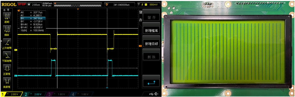
An experimental example of display interface MCU 8080/6800:
A LCD controller has been phased out, and the customer would like to have a pin-to-pin compatible module to replace it. RD owners had designed a PCB with an MCU for the compatible interface. The experimental results on ENABLE signal must be as long as 9.92uS at least. This means the maximum communication BW is around 100KBPS.
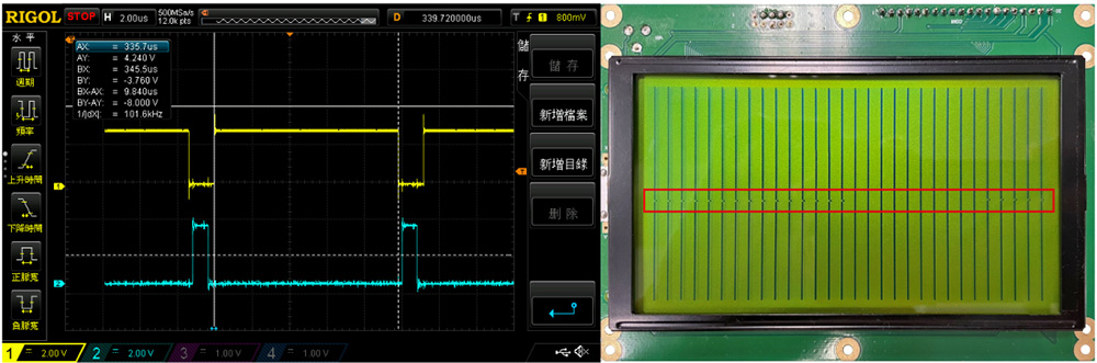
We can see a few defect points below when shortening ENABLE time as 9.84uS (the communication speed is up to 101KBPS).
A comparison table on display interface:
Which interface is the best? There is no absolute answer to this question. The users should choose the suitable interface for their applications, not the best. Let's see the following comparison of the pros and cons of these interfaces.
| Display Interface | Resolution | Speed | Pin Count. | Noise | Power Consumption | Connect Distance | Cost |
|---|---|---|---|---|---|---|---|
| MCU 8080/6800 | Middle | Low | More | Middle | Low | Short | Low |
| RGB 16/18/24 | Middle | Fast | More | Worst | High | Short | Low |
| SPI | Small | Low | Less | Middle | Low | Short | Low |
| I²C | Small | Low | Less | Middle | Low | Short | Low |
| Serial RGB 6/8 | Middle | Fast | Less | Worst | High | Short | Low |
| LVDS | Large | Fast | Less | Best | Low | Long | High |
| MIPI | Large | Fastest | Less | Best | Low | Short | Average |