


3.12" 256x64 COF Touch OLED Display with PCB +Frame
Model No. WEN025664B-CTP
►Graphic OLED Display
►3.12" OLED
►Structure: COF+FR+PCB
►256×64 Dot Matrix
►IC:SSD1322
►3V power supply
►1/64 duty cycle
►Interface: 6800, 8080, SPI
►With Capacitive Touch Screen (CTP)
►Detect Point : 1 Finger
►Display Color: White / Yellow / Sky Blue / Green
►Support Grayscale
Description
WEN025664B-CTP model is a COF Graphic OLED with Capacitive Touch, featuring a diagonal size of 3.12 inches and a resolution of 256x64 dots. This OLED module is built-in with the SSD1322 IC and supports 8-bits 6800/8080 and 3/4-line SPI interfaces. It also supports 4-bits grayscale, with a logic supply voltage of 3V. The display's current at 50% check board is 150mA @3.0V VDD (typical value), with a driving duty of 1/64. The model includes a capacitive touch panel with the FT6336U IC supporting an I2C interface, one detect point for CTP, and a normal glare surface glass.
The module has a built-in PCB, allowing customers to use wire connections without the need for additional PCB development for their applications. Additionally, the integrated VCC circuit on the PCB simplifies customer usage. This PCB board, equipped with four mounting holes, provides an easy method for customers to secure modules in their applications. This OLED module is suitable for smart home applications, medical devices, industrial control, etc.
The WEN025664B-CTP model can operate at temperatures ranging from -20℃ to +70℃, with storage temperatures ranging from -30℃ to +80℃. The OLED module features a high contrast ratio of 10,000:1, resulting in enhanced image quality, sharper details, and improved readability, especially in low-light environments.
Additionally, the product line of the same OLED panels offers various alternatives:- WEX025664B series without a metal frame, PCB, and touch screen.
- WEX025664B-CTP series without a metal frame, PCB, and with a CTP touch screen.
- WEN025664B series with a metal frame and PCB.
DRAWING
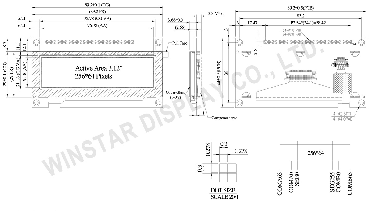
Data source ref: WEN025664BWPP3D00000
SPECIFICATIONS
Interface Pin Function
| Pin Number | Symbol | I/O | Function | ||||||||||
|---|---|---|---|---|---|---|---|---|---|---|---|---|---|
| 1 | VSS | P | Ground. | ||||||||||
| 2 | VDD | P | Power Supply for Core Logic Circuit Power supply pin for core logic operation. A capacitor is required to connect between this pin and VSS |
||||||||||
| 3 | N.C. | P | Reserved Pin The N.C. pin between function pins are reserved for compatible and flexible design. |
||||||||||
| 4 | D/C# | I | Data/Command Control This pin is Data/Command control pin connecting to the MCU. When the pin is pulled HIGH, the content at D[7:0] will be interpreted as data. When the pin is pulled LOW, the content at D[7:0] will be interpreted as command. |
||||||||||
| 5 | R/W# (WR#) |
I | Read/Write Select or Write This pin is MCU interface input. When interfacing to a 68XX-series microprocessor, this pin will be used as Read/Write (R/W#) selection input. Pull this pin to “High” for read mode and pull it to “Low” for write mode. When 80XX interface mode is selected, this pin will be the Write (WR#) input. Data write operation is initiated when this pin is pulled low and the CS# is pulled low. When serial mode is selected, this pin must be connected to VSS. |
||||||||||
| 6 | E/RD# | I | Read/Write Enable or Read This pin is MCU interface input. When interfacing to a 68XX-series microprocessor, this pin will be used as the Enable (E) signal. Read/write operation is initiated when this pin is pulled high and the CS# is pulled low. When connecting to an 80XX-microprocessor, this pin receives the Read (RD#) signal. Data read operation is initiated when this pin is pulled low and CS# is pulled low. When serial mode is selected, this pin must be connected to VSS. |
||||||||||
| 7~14 | DB0 | I/O | Host Data Input/Output Bus These pins are 8-bit bi-directional data bus to be connected to the microprocessor’s data bus. When serial mode is selected, D1 will be the serial data input SDIN and D0 will be the serial clock input SCLK. |
||||||||||
| DB1 | |||||||||||||
| DB2 | |||||||||||||
| DB3 | |||||||||||||
| DB4 | |||||||||||||
| DB5 | |||||||||||||
| DB6 | |||||||||||||
| DB7 | |||||||||||||
| 15 | NC | P | Reserved Pin The N.C. pin between function pins are reserved for compatible and flexible design. |
||||||||||
| 16 | RES# | I | This pin is reset signal input. When the pin is pulled LOW, initialization of the chip is executed. Keep this pin pull HIGH during normal operation. |
||||||||||
| 17 | CS# | I | Data/Command Control This pin is the chip select input connecting to the MCU. The chip is enabled for MCU communication only when CS# is pulled LOW. |
||||||||||
| 18 | NC | P | Reserved Pin The N.C. pin between function pins are reserved for compatible and flexible design. |
||||||||||
| 19 | BS1 | I | Communicating Protocol Select These pins are MCU interface selection input. See the following table:
(1) 0 is connected to VSS (2) 1 is connected to VDD |
||||||||||
| 20 | BS0 | ||||||||||||
| 21 | TP_SCK | I | I2C clock input | ||||||||||
| 22 | TP_SDA | I | I2C data input and output | ||||||||||
| 23 | TP_INT | I | External interrupt to the host | ||||||||||
| 24 | TP_RST | I | External Reset, Low is active |
General Specification
| Item | Dimension | Unit |
|---|---|---|
| Dot Matrix | 256 x 64 Dots | - |
| Module dimension | 89.2 × 44.0 × 7.98 | mm |
| Active Area | 76.78 × 19.18 | mm |
| Pixel Size | 0.278 × 0.278 | mm |
| Pixel Pitch | 0.3 × 0.3 | mm |
| Display Mode | Passive Matrix | |
| Display Color | Monochrome | |
| Drive Duty | 1/64 Duty | |
| Gray Scale | 4 bits | |
| OLED IC | SSD1322 (COF) | |
| OLED Interface | 6800, 8080, SPI | |
| Size | 3.12 inch | |
| CTP IC | FT6336U | |
| Detect Point | 1 | |
| CTP Interface | I2C | |
| Surface | Normal Glare | |
Absolute Maximum Ratings
| Parameter | Symbol | Min | Max | Unit |
|---|---|---|---|---|
| Supply Voltage for Display | VDD | -0.3 | 4 | V |
| Operating Temperature | TOP | -20 | +70 | °C |
| Storage Temperature | TSTG | -30 | +80 | °C |
Electronical Characteristics
DC Electrical Characteristics
| Item | Symbol | Condition | Min | Typ | Max | Unit |
|---|---|---|---|---|---|---|
| Supply Voltage for Logic | VDD | - | 2.8 | 3.0 | 3.3 | V |
| High Level Input | VIH | - | 0.8×VDD | - | VDD | V |
| Low Level Input | VIL | - | 0 | - | 0.2×VDD | V |
| High Level Output | VOH | - | 0.9×VDD | - | VDD | V |
| Low Level Output | VOL | - | 0 | - | 0.1×VDD | V |
| 50% Check Board operating Current | IDD | VDD =3V | - | 150 | 300 | mA |
Search keyword: 256x64 oled, oled 256x64, 3.12 oled, 3.12" oled, 3.12 inch oled, oled 3.12, oled 3.12"
