


2.8-Inch Grayscale COF OLED Display with 256x64 Resolution, Touch Panel, PCB, and Frame Support
Model No. WEN025664A-CTP
►Graphic OLED Display
►2.8" OLED
►Structure: COF + Frame + PCB
►256×64 Dot Matrix
►IC:SSD1322
►3V power supply
►1/64 duty cycle
►Interface: 6800, 8080, SPI
►With Capacitive Touch Screen (CTP)
►Detect Point : 1 Finger
►Display Color: White / Yellow
►Support Grayscale
Description
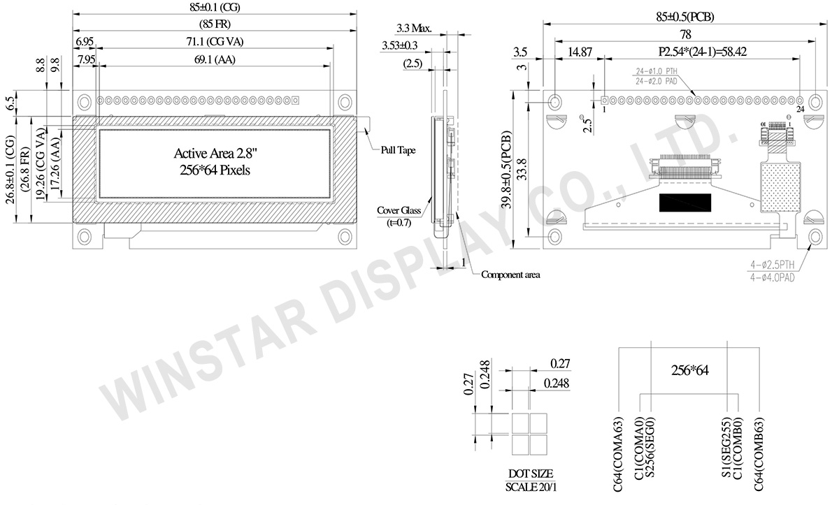
The WEN025664A-CTP series is a 2.8-inch monochrome graphic COF OLED display featuring a capacitive touch panel with a resolution of 256x64 dots. It is equipped with the SSD1322 IC and supports multiple interfaces, including 6800/8080 8-bit and 3/4-wire SPI interfaces. The module dimensions of the WEN025664A-CTP are 85.0 × 39.8 mm, and the active area is 69.1 × 17.26 mm. The model incorporates a projected capacitive touch panel (PCAP) with the FT6336U IC, supporting I2C interfaces and 1-point touch.
The WEN025664A-CTP OLED series operates on a 3V power supply with a driving method of 1/64 duty. It supports grayscales and boasts a high contrast ratio of 10,000:1. The module is capable of functioning in temperatures ranging from -20°C to +70°C, with a storage temperature range of -30°C to +80°C.
Featuring a metal frame with a PCB board and four screw holes, the WEN025664A-CTP facilitates easy installation for customers. The OLED series, equipped with a PCB board, can effortlessly connect with applications using wires, eliminating the need for customers to develop additional PCB boards. The integration of interface settings and VDD circuits enhances user-friendliness. Additionally, the four screw holes on the PCB simplify the installation process onto the application product.
The WEN025664A-CTP series also offers an option with the same OLED panel but without a touch panel. Please choose the WEN025664A series for the non-touch panel option.
DRAWING
Data source ref: WEN025664AWPP3D00000
SPECIFICATIONS
Interface Pin Function
| Pin Number | Symbol | I/O | Function | ||||||||||
|---|---|---|---|---|---|---|---|---|---|---|---|---|---|
| 1 | VSS | P | Ground. | ||||||||||
| 2 | VDD | P | Power Supply for Core Logic Circuit Power supply pin for core logic operation. A capacitor is required to connect between this pin and VSS |
||||||||||
| 3 | N.C. | P | Reserved Pin The N.C. pin between function pins are reserved for compatible and flexible design. |
||||||||||
| 4 | D/C# | I | Data/Command Control This pin is Data/Command control pin connecting to the MCU. When the pin is pulled HIGH, the content at D[7:0] will be interpreted as data. When the pin is pulled LOW, the content at D[7:0] will be interpreted as command. |
||||||||||
| 5 | R/W# (WR#) |
I | Read/Write Select or Write This pin is MCU interface input. When interfacing to a 68XX-series microprocessor, this pin will be used as Read/Write (R/W#) selection input. Pull this pin to “High” for read mode and pull it to “Low” for write mode. When 80XX interface mode is selected, this pin will be the Write (WR#) input. Data write operation is initiated when this pin is pulled low and the CS# is pulled low. When serial mode is selected, this pin must be connected to VSS. |
||||||||||
| 6 | E/RD# | I | Read/Write Enable or Read This pin is MCU interface input. When interfacing to a 68XX-series microprocessor, this pin will be used as the Enable (E) signal. Read/write operation is initiated when this pin is pulled high and the CS# is pulled low. When connecting to an 80XX-microprocessor, this pin receives the Read (RD#) signal. Data read operation is initiated when this pin is pulled low and CS# is pulled low. When serial mode is selected, this pin must be connected to VSS. |
||||||||||
| 7~14 | DB0 | I/O | Host Data Input/Output Bus These pins are 8-bit bi-directional data bus to be connected to the microprocessor’s data bus. When serial mode is selected, D1 will be the serial data input SDIN and D0 will be the serial clock input SCLK. |
||||||||||
| DB1 | |||||||||||||
| DB2 | |||||||||||||
| DB3 | |||||||||||||
| DB4 | |||||||||||||
| DB5 | |||||||||||||
| DB6 | |||||||||||||
| DB7 | |||||||||||||
| 15 | NC | P | Reserved Pin The N.C. pin between function pins are reserved for compatible and flexible design. |
||||||||||
| 16 | RES# | I | This pin is reset signal input. When the pin is pulled LOW, initialization of the chip is executed. Keep this pin pull HIGH during normal operation. |
||||||||||
| 17 | CS# | I | Data/Command Control This pin is the chip select input connecting to the MCU. The chip is enabled for MCU communication only when CS# is pulled LOW. |
||||||||||
| 18 | NC | P | Reserved Pin The N.C. pin between function pins are reserved for compatible and flexible design. |
||||||||||
| 19 | BS1 | I | Communicating Protocol Select These pins are MCU interface selection input. See the following table:
Note (1) 0 is connected to VSS (2) 1 is connected to VDD |
||||||||||
| 20 | BS0 | ||||||||||||
| 21 | TP_SCK | I | I2C clock input | ||||||||||
| 22 | TP_SDA | I | I2C data input and output | ||||||||||
| 23 | TP_INT | I | External interrupt to the host | ||||||||||
| 24 | TP_RST | I | External Reset, Low is active |
General Specification
| Item | Dimension | Unit |
|---|---|---|
| Dot Matrix | 256 × 64 Dots | - |
| Module dimension | 85.0 × 39.8 ×7.83 | mm |
| Active Area | 69.1 × 17.26 | mm |
| Pixel Size | 0.248×0.248 | mm |
| Pixel Pitch | 0.27×0.27 | mm |
| Display Mode | Passive Matrix | |
| Display Color | Monochrome | |
| Drive Duty | 1/64 Duty | |
| OLED IC | SSD1322 (COF) | |
| OLED Interface | 6800, 8080, SPI | |
| Size | 2.8 inch | |
| CTP IC | FT6336U | |
| Detect Point | 1 | |
| CTP Interface | I2C | |
| Surface | Normal Glare | |
Absolute Maximum Ratings
Absolute Maximum Ratings
| Parameter | Symbol | Min | Max | Unit |
|---|---|---|---|---|
| Supply Voltage for Display | VDD | -0.3 | 4 | V |
| Operating Temperature | TOP | -20 | +70 | °C |
| Storage Temperature | TSTG | -30 | +80 | °C |
Electronical Characteristics
DC Electrical Characteristics
| Item | Symbol | Condition | Min | Typ | Max | Unit |
|---|---|---|---|---|---|---|
| Supply Voltage for Logic | VDD | - | 2.8 | 3.0 | 3.3 | V |
| High Level Input | VIH | - | 0.8×VDD | - | VDD | V |
| Low Level Input | VIL | - | 0 | - | 0.2×VDD | V |
| High Level Output | VOH | - | 0.9×VDD | - | VDD | V |
| Low Level Output | VOL | - | 0 | - | 0.1×VDD | V |
| 50% Check Board operating Current | IDD | VDD =3V | - | 125 | 250 | mA |
Search keyword: 256x64 oled, oled 256x64, 2.8 oled, 2.8" oled, 2.8 inch oled, oled 2.8, oled 2.8"
