


16x2 COG 1.23" OLED Character Display with WS0012 IC
Model No. WEO001602H
►Type : Character
►Structure : COG
►16 characters x 2 Lines
►IC:WS0012
►3.3V Power supply
►1/16 duty
►Interface: 6800, 8080, SPI, I2C
►Display Color: White / Yellow
Description
WEO001602H is a16 Character x 2 lines COG OLED display module. This 16x2 OLED display is built-in with WS0012 IC; it supports 6800/8080 8-bit parallel and I2C, 4-wire SPI interface, the supply voltage for logic is 3.3V (VDD), and the supply voltage for display is 8.5V(VCC). The current with 50% checkerboard display is 2mA @ VCC 8.5V (for white color), 1/16 driving duty. WEO001602H OLED module can be operating at temperatures from -40℃ to +80℃; its storage temperatures range from -40℃ to +85℃.
We suggest customers consider using this low-power 16x2 character OLED to upgrade the existing STN character display. Below are the advantages of this OLED display.
►Faster response time "At +25 ℃ 10 μsec
►Unlimited viewing angle "Up to 175 degree
►Thin – No need of backlight, self-emitting
►High Brightness
►High contrast ratio 10,000:1
►Wide Operation Temperature
►Lower power consumption
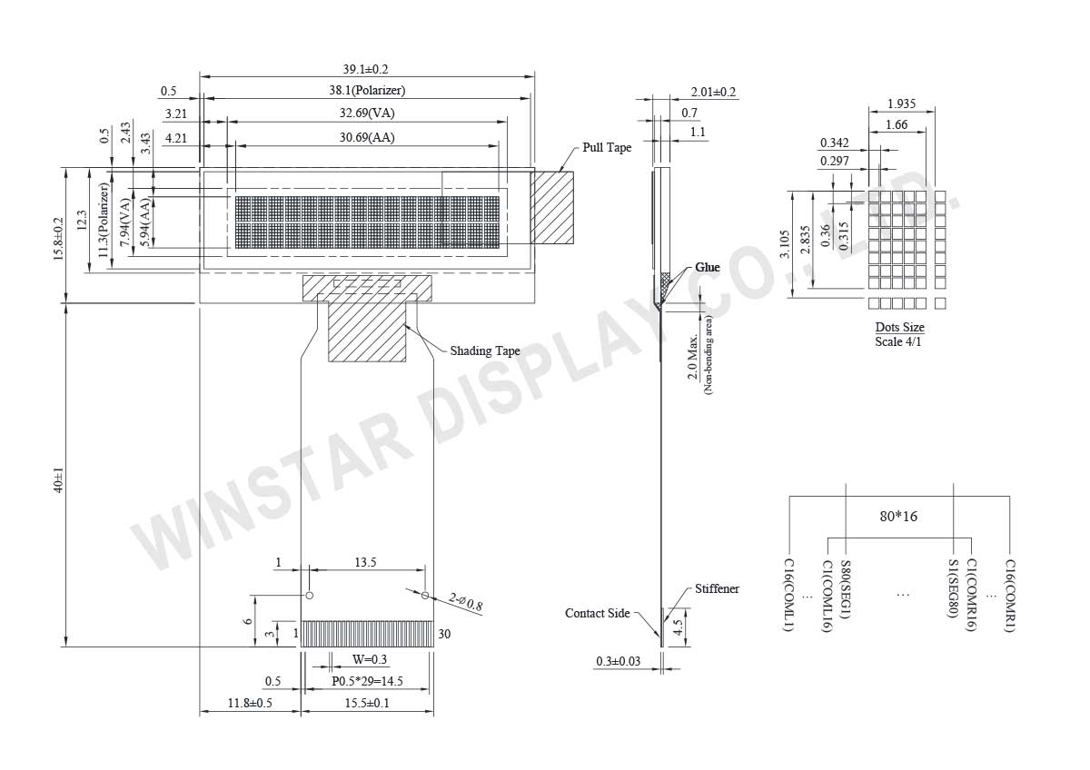
DRAWING
SPECIFICATIONS
Interface Pin Function
| Pin No. | Symbol | Level | Description | |||||||||||||||
|---|---|---|---|---|---|---|---|---|---|---|---|---|---|---|---|---|---|---|
| 1 | GND | P | Ground Pin | |||||||||||||||
| 2 | V16 | I | This is the most positive voltage supply pin of the chip. It can be supplied externally or generated internally by using internal DC-DC voltage converter. | |||||||||||||||
| 3 | VCI | P | DCDC buffer Power Supply | |||||||||||||||
| 4 | GND | P | Ground Pin | |||||||||||||||
| 5 | VCC | P | Power Pin | |||||||||||||||
| 6 | BVR | I | Brightness control pin. It should be connected to VCC. | |||||||||||||||
| 7 | DVR | I | Pre charge time control. It should be connected to VCC. | |||||||||||||||
| 8 | VBREF | O | This pin is the internal voltage reference of DCDC1 circuit. A stabilization capacitor should be connected between this pin and GND | |||||||||||||||
| 9 | RESE | I | NMOS source input pin: This pin connects to the source current pin of the external NMOS of the booster circuit. |
|||||||||||||||
| 10 | GDR | O | Gate drive pulse output pin: This output pin drives the gate of external NMOS of the booster circuit. |
|||||||||||||||
| 11 | FB | I | Feedback voltage input pin: This pin is the feedback resistor input of the booster circuit. It is used to adjust the booster output voltage level. |
|||||||||||||||
| 12 | VDD | P | Power Pin (connect to stabilization capacitor) | |||||||||||||||
| 13 | IM1 | I | Interface selection
|
|||||||||||||||
| 14 | IM0 | I | ||||||||||||||||
| 15 | RESETB | I | Reset pin | |||||||||||||||
| 16 | RS | I | Register Select Input Pin When this pin is set to "0", it is used as an Instruction Register. When this pin is set to "1", it is used for as the Data Register. |
|||||||||||||||
| 17 | CSB | I | Chip select input pins Data / instruction I/O is enabled only when CSB is “L”. |
|||||||||||||||
| 18 | RDB | I | Read / Write execution control pin
|
|||||||||||||||
| 19 | WRB | I | Read / Write execution control pin
|
|||||||||||||||
| 20 | SDA | I/O | SDA is the serial data input for I2C. | |||||||||||||||
| 21 | SDC | I/O | SDC is the serial clock input/output for I2C. | |||||||||||||||
| 22~25 | DB7~DB4 | I/O | High Order Bidirectional Data I/O Pins These pins are used for data transfer and reception between the MPU and WS0012. When SPI is selected, DB5 will be the serial clock input: SCL DB7 will be the serial data input: SDI. DB6 will be the serial data output: SDO. |
|||||||||||||||
| 26~29 | DB3~DB0 | I/O | Low Order Bidirectional Data I/O Pins These pins are used for data transfer and reception between the MPU and WS0012. These pins are not used during a 4-bit operation. |
|||||||||||||||
| 30 | GND | P | Ground Pin |
Mechanical Data
| Item | Dimension | Unit |
|---|---|---|
| Number of Characters | 16 characters x 2 Lines | - |
| Module dimension | 39.1 x 15.8 x 2.01 | mm |
| View area | 32.69 x 7.94 | mm |
| Active area | 30.69 x 5.94 | mm |
| Dot size | 0.297 x 0.315 | mm |
| Dot pitch | 0.342 x 0.36 | mm |
| Character size | 1.66 x 2.835 | mm |
| Character pitch | 1.935 x 3.105 | mm |
| Panel type | OLED , Monochrome | |
| Duty | 1/16 | |
| IC | WS0012 | |
| Interface | 6800, 8080, SPI, I2C | |
| Size | 1.23 inch | |
Absolute Maximum Ratings
| Item | Symbol | Min | Max | Unit |
|---|---|---|---|---|
| Operating Temperature | TOP | -40 | +80 | °C |
| Storage Temperature | TST | -40 | +85 | °C |
| Supply Voltage For Logic | VCC | -0.3 | 3.6 | V |
| Supply Voltage For DCDC converter | VCI | -0.3 | 3.6 | V |
| Supply Voltage for Display | V16 | -0.3 | 19.0 | V |
Electronical Characteristics
DC Electrical Characteristics
| Item | Symbol | Condition | Min | Typ | Max | Unit |
|---|---|---|---|---|---|---|
| Supply Voltage For Logic | VCC | - | 2.6 | 3.3 | 3.5 | V |
| Supply Voltage For DCDC converter | VCI | - | 2.6 | 3.3 | 3.5 | V |
| Supply Voltage for Display | V16 | - | - | 12.5 | 13.0 | V |
| Input High Volt. | VIH | - | 0.9xVCC | - | VCC | V |
| Input Low Volt. | VIL | - | GND | - | 0.1xVCC | V |
| Output High Volt. | VOH | IOH=-0.5mA | 0.8xVCC | - | VCC | V |
| Output Low Volt. | VOL | IOL=0.5mA | GND | - | 0.2xVCC | V |
| 50% Checkerboard Operating Current |
I16 | V16=12.5V | - | 2 | 4 | mA |
