

1920x720 IPS TFT Display 12.3" with Capacitive Touch
Model No. WF123BSWAYLNBA
►Size: 12.3"
►Resolution : 1920x720 dots
►View Direction :85/85/85/85 (IPS)
►Interface :2ch-LVDS
►Driver IC :HX8298-C01-LT+HX8695-E-LT
►Control-Board : No
►Brightness (cd/m²): 650
►Frame Through Hole : No
►Touch Screen : Projected Capacitive Touch Panel (PCAP)
►Detect Point : 10 Fingers
►Operating Temperature: -30~+85℃
Description
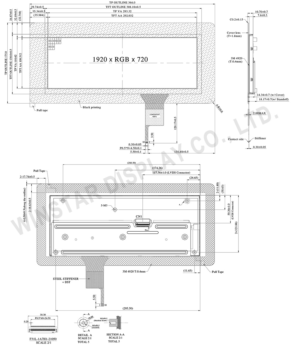
WF123BSWAYLNBA is a 12.3-inch touch TFT display with IPS 85/85/85/85 wide viewing angles. It has 1920x720 dots resolution and 650 cd/m2 brightness. The module dimension is 364.0(H) × 175.0 (V) mm, and the active area is 292.032(H) × 109.512(V) mm. The module is built-in with HX8298-C01-LT+HX8695-E-LT driver IC, supporting 2ch-LVDS interfaces. It comes with a Projected Capacitive Touch Panel (PCAP), which can simultaneously detect 10 points of contact.
The supply voltage (VCC) of the display is from 3V to 3.6V, with a typical value of 3.3V. This TFT can operate at temperatures from -30℃ to +85 ℃, and its storage temperatures are from -40 to +90 ℃.
The supply voltage (VCC) of the display is from 3V to 3.6V, with a typical value of 3.3V. This TFT can operate at temperatures from -30℃ to +85 ℃, and its storage temperatures are from -40 to +90 ℃.
DRAWING
SPECIFICATIONS
Interface
TFT LCD Module
FPC connector is used for electronics interface.
AORORA F31L-1A7H1-21050 , 50PIN
| Pin no. | Symbol | Function |
|---|---|---|
| 1 | GND | Ground |
| 2 | NC | No connector |
| 3 | VCC | Digital Power |
| 4 | VCC | Digital Power |
| 5 | GND | Panel Power |
| 6 | GND | Panel Power |
| 7 | NC | No connector |
| 8 | NC | No connector |
| 9 | GND | Ground |
| 10 | ORXIN0- | Odd pixel negative LVDS differential clock input |
| 11 | ORXIN0+ | Odd pixel positive LVDS differential clock input |
| 12 | ORXIN1- | Odd pixel negative LVDS differential clock input |
| 13 | ORXIN1+ | Odd pixel positive LVDS differential clock input |
| 14 | ORXIN2- | Odd pixel negative LVDS differential clock input |
| 15 | ORXIN2+ | Odd pixel positive LVDS differential clock input |
| 16 | ORXCLKIN- | Odd pixel negative LVDS differential clock input |
| 17 | ORXCLKIN+ | Odd pixel positive LVDS differential clock input |
| 18 | ORXIN3- | Odd pixel negative LVDS differential clock input |
| 19 | ORXIN3+ | Odd pixel positive LVDS differential clock input |
| 20 | ERXIN0- | Even pixel negative LVDS differential clock input |
| 21 | ERXIN0+ | Even pixel positive LVDS differential clock input |
| 22 | ERXIN1- | Even pixel negative LVDS differential clock input |
| 23 | ERXIN1+ | Even pixel positive LVDS differential clock input |
| 24 | ERXIN2- | Even pixel negative LVDS differential clock input |
| 25 | ERXIN2+ | Even pixel positive LVDS differential clock input |
| 26 | ERXCLKIN- | Even pixel negative LVDS differential clock input |
| 27 | ERXCLKIN+ | Even pixel positive LVDS differential clock input |
| 28 | ERXIN3- | Even pixel negative LVDS differential clock input |
| 29 | ERXIN3+ | Even pixel positive LVDS differential clock input |
| 30 | GND | Ground |
| 31 | NC | No connector |
| 32 | RESETB | Global reset pin, active low. |
| 33 | STBYB | Standby mode, active low. |
| 34 | CA3 | Output signal to indicate self protection mode, when DE,HS,VS,DCLK, any of these signals is missing, it will become High. If using this pin, CA3 need to pulled low by an resistor,else , let it floating. |
| 35 | SCL | Serial interface clock input. (User folating) |
| 36 | SDA | Serial interface data input/output.(User folating) |
| 37 | CSB | Serial interface chip enable.(User folating) |
| 38 | GND | Power Ground |
| 39 | GND | Power Ground |
| 40 | NC | No connector |
| 41 | LEDA | LED power (Anode) |
| 42 | LEDA | LED power (Anode) |
| 43 | LEDA | LED power (Anode) |
| 44 | NC | No connector |
| 45 | LEDK1 | Cathode 1 |
| 46 | LEDK2 | Cathode 2 |
| 47 | LEDK3 | Cathode 3 |
| 48 | LEDK4 | Cathode 4 |
| 49 | NTC_A | NTC_Anode |
| 50 | NTC_K | NTC_Cathode |
PCAP PIN Definition
| Pin | Symbol | Function |
|---|---|---|
| 1 | USB_VSS | System ground |
| 2 | USB_VDD 5V | Power supply |
| 3 | USB_D+ | Data + |
| 4 | USB_D- | Data - |
| 5 | VSS | System ground |
| 6 | SDA | I2C data input and output |
| 7 | SCL | I2C clock input |
| 8 | RST | External Reset, Low is active |
| 9 | INT | External interrupt to the host |
| 10 | VDDT 3.3 | Power supply |
General Specifications
| Item | Dimension | Unit |
|---|---|---|
| Size | 12.3 | inch |
| Pixel Number | 1920 RGB (H) × 720(V) | pixel |
| Module dimension | 364.0(H) × 175.0 (V) × 10.7 | mm |
| Active Area | 292.032(H) × 109.512(V) | mm |
| Pixel Pitch | 0.1521(H) × 0.1521 (V) | mm |
| LCD type | TFT, Normally Black, Transmissive | |
| Driver IC | HX8298-C01-LT+HX8695-E-LT or Equivalent | |
| Viewing Angle | 85/85/85/85 | |
| Backlight Type | LED ,Normally White | |
| TFT Interface | 2ch-LVDS | |
| PCAP IC | ILI2511 or equivalent | |
| PCAP Interface | USB (I2C available) | |
| PCAP FW Version | V6.0.0.0.0.0.0.3 | |
| Touch Panel | Projected Capacitive Touch Screen, PCAP | |
| Surface | Glare | |
Absolute Maximum Ratings
| Item | Symbol | Min | Typ | Max | Unit |
|---|---|---|---|---|---|
| Operating Temperature | TOP | -30 | - | +85 | ℃ |
| Storage Temperature | TST | -40 | - | +90 | ℃ |
Electrical Characteristics
| Item | Symbol | Min. | Typ. | Max. | Unit |
|---|---|---|---|---|---|
| Supply Voltage | VCC | 3 | 3.3 | 3.6 | V |
| Input signal voltage | ViH | VCC *0.7 | - | VCC | V |
| ViL | 0 | - | VCC *0.3 | V | |
| Current of power supply | ICC | - | - | 500 | mA |
| Inrush current | IRUSH | - | - | 2.0 | A |
| Supply CTP(USB) | USB_VDD 5V | 4.75 | 5.0 | 5.25 | V |
| I USB_VDD | - | 90 | 135 | mA | |
| Supply CTP(I2C) | VDDT 3.3 | 3.15 | 3.3 | 3.45 | V |
| IVDDT | - | 90 | 135 | mA |
Search keyword: tft 12.3, tft 12.3", 12.3 tft lcd, 12.3" tft lcd, 12.3 inch tft lcd, tft lcd 12.3, 12.3 tft display,12.3" tft display, 12.3 inch tft display, tft display 12.3, tft display 12.3"
