


2.7", 128x64 COG Capacitive Touch OLED Display with Frame +PCB
Model No. WEP012864U-CTP
►Type: Graphic
►Structure: COG + Frame + PCB
►Size: 2.7 inch
►128 x 64 Dot Matrix
►IC:SSD1357
►3V Power supply
►1/64 duty
►Interface: 6800, 8080, SPI, I2C
►With Capacitive Touch Screen (CTP)
►Detect Point : 1 Finger
►Display Color: White / Yellow
►Support Grayscale
Description
WEP012864U-CTP is a COG graphic OLED display featuring a capacitive touch panel with a resolution of 128x64 dots and a 2.7-inch (61.41 × 30.69 mm) active area. The module is equipped with the SSD1357 IC, supporting 6800/8080 8-bit and 4-wire SPI, as well as I2C interfaces. The display supports 4-bit grayscale, with a logic voltage of 3V and a duty cycle of 1/64. The capacitive touch panel includes the built-in IC GT911, supporting an I2C interface with 1-point touch capability.
The WEP012864U-CTP OLED series comes with a metal frame and a PCB board that easily connects to the application via wires. Customers are not required to develop additional PCB boards themselves, as it integrates interface settings and VCC circuits, simplifying the user experience. The PCB is designed with four screw holes for easy installation of the module on the application product.
This OLED module boasts a high contrast ratio of 10,000:1, allowing for more vibrant and deeper blacks, as well as brighter whites. This leads to enhanced image quality, sharper details, and improved readability. The module is operational within a temperature range of -20℃ to 70℃, with storage temperatures spanning from -30℃ to 80℃.
WEP012864U, featuring a CTP touch panel, is highly suitable for smart home applications, hi-tech equipment, meter equipment, industrial control systems, medical instruments, and more.
DRAWING
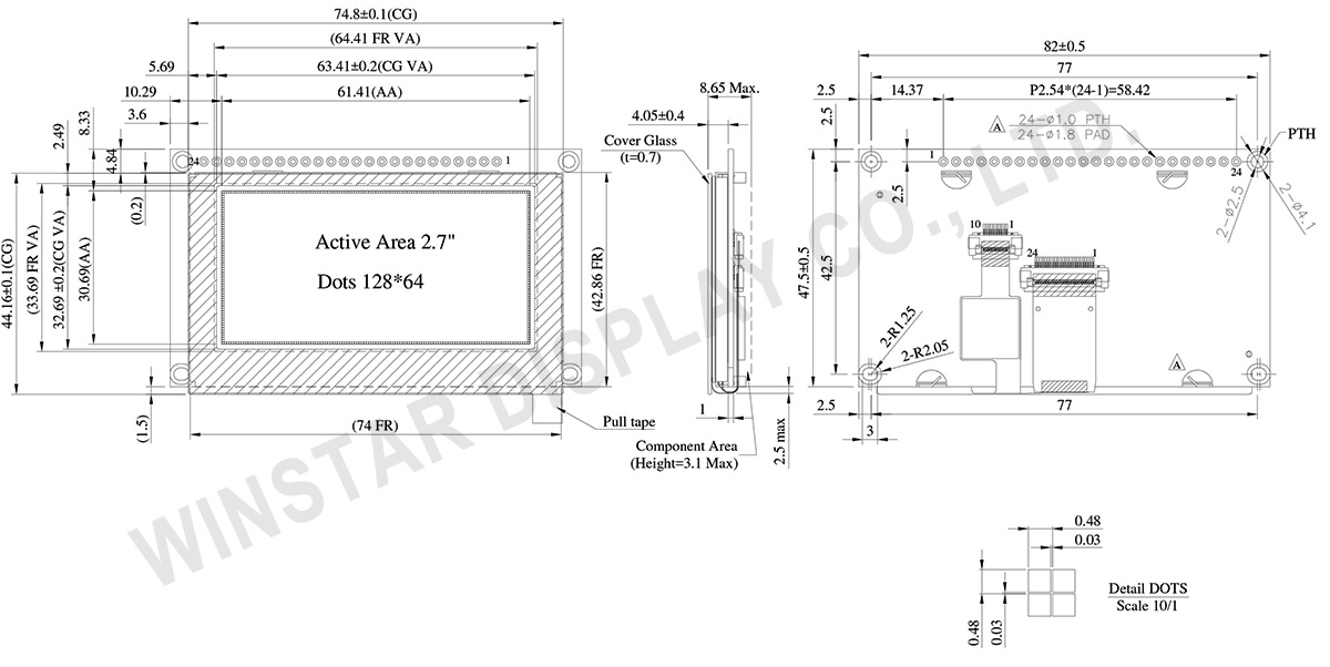
Data source ref: WEP012864UWPP3D00000
SPECIFICATIONS
Interface Pin Function
| No. | Symbol | Function | |||||||||||||||
|---|---|---|---|---|---|---|---|---|---|---|---|---|---|---|---|---|---|
| 1 | VSS | This is a ground pin. | |||||||||||||||
| 2 | VDD | Power supply pin for core logic operation | |||||||||||||||
| 3 | NC | Reserved Pin The N.C. pin between function pins is reserved for compatible and flexible design. |
|||||||||||||||
| 4 | D/C# | This pin is Data/Command control pin connecting to the MCU. When the pin is pulled HIGH, the data at D[7:0] will be interpreted as data. When the pin is pulled LOW, the data at D[7:0] will be transferred to a command register. In I2C mode, this pin acts as SA0 for slave address selection. When 3-wire serial interface is selected, this pin must be connected to VSS. |
|||||||||||||||
| 5 | R/W# (WR#) |
This pin is read / write control input pin connecting to the MCU interface. When 6800 interface mode is selected, this pin will be used as Read/Write (R/W#) selection input. Read mode will be carried out when this pin is pulled HIGH and write mode when LOW. When 8080 interface mode is selected, this pin will be the Write (WR#) input. Data write operation is initiated when this pin is pulled LOW and the chip is selected. When serial or I2C interface is selected, this pin must be connected to VSS. |
|||||||||||||||
| 6 | E/RD# | This pin is MCU interface input. When 6800 interface mode is selected, this pin will be used as the Enable (E) signal. Read/write operation is initiated when this pin is pulled HIGH and the chip is selected. When 8080 interface mode is selected, this pin receives the Read (RD#) signal. Read operation is initiated when this pin is pulled LOW and the chip is selected. When serial or I2C interface is selected, this pin must be connected to VSS. |
|||||||||||||||
| 7 | DB0 | These pins are bi-directional data bus connecting to the MCU data bus. Unused pins are recommended to tie LOW. When serial interface mode is selected, D0 will be the serial clock input: SCLK; D1 will be the serial data input: SDIN. When I2C mode is selected, D2, D1 should be tied together and serve as SDAout, SDAin in application and D0 is the serial clock input, SCL. |
|||||||||||||||
| 8 | DB1 | ||||||||||||||||
| 9 | DB2 | ||||||||||||||||
| 10 | DB3 | ||||||||||||||||
| 11 | DB4 | ||||||||||||||||
| 12 | DB5 | ||||||||||||||||
| 13 | DB6 | ||||||||||||||||
| 14 | DB7 | ||||||||||||||||
| 15 | NC | No connection | |||||||||||||||
| 16 | RES# | This pin is reset signal input. When the pin is pulled LOW, initialization of the chip is executed. Keep this pin pull HIGH during normal operation. |
|||||||||||||||
| 17 | CS# | Chip Select This pin is the chip select input. The chip is enabled for MCU communication only when CS# is pulled low. |
|||||||||||||||
| 18 | NC | No connection | |||||||||||||||
| 19 | BS2 | Communicating Protocol Select. These pins are MCU interface selection input. See the following table:
|
|||||||||||||||
| 20 | BS1 | ||||||||||||||||
| 21 | TP_SCK | I2C clock signal | |||||||||||||||
| 22 | TP_SDA | I2C data signal | |||||||||||||||
| 23 | TP_INT | Interrupt signal, active low, asserted to request Host start a new transaction |
|||||||||||||||
| 24 | TP_RST | External reset signal, active low |
Mechanical Data
| Item | Dimension | Unit |
|---|---|---|
| Dot Matrix | 128 x 64 | - |
| Module dimension | 82.0 × 47.5 × 8.65 Max. | mm |
| Active Area | 61.41 × 30.69 | mm |
| Pixel Size | 0.45 × 0.45 | mm |
| Pixel Pitch | 0.48 × 0.48 | mm |
| Display Mode | Passive Matrix | |
| Display Color | Monochrome | |
| Drive Duty | 1/64 Duty | |
| Gray Scale | 4 bits | |
| IC | SSD1357 | |
| Interface | 8-bits 6800 and 8080 parallel, 4-line SPI, I2C | |
| Size | 2.7 inch | |
| CTP IC | GT911 |
| Detect Point | 1 |
| CTP Interface | I2C |
| Surface | Normal Glare |
Absolute Maximum Ratings
| Parameter | Symbol | Min | Max | Unit |
|---|---|---|---|---|
| Supply Voltage for Logic | VDD | -0.3 | 4.0 | V |
| Operating Temperature | TOP | -20 | +70 | °C |
| Storage Temperature | TSTG | -30 | +80 | °C |
Electronical Characteristics
DC Electrical Characteristics
| Item | Symbol | Condition | Min | Typ | Max | Unit |
|---|---|---|---|---|---|---|
| Supply Voltage for Logic | VDD | - | 2.8 | 3.0 | 3.3 | V |
| High Level Input | VIH | - | 0.8×VDD | - | - | V |
| Low Level Input | VIL | - | - | - | 0.2×VDD | V |
| High Level Output | VOH | - | 0.9×VDD | - | - | V |
| Low Level Output | VOL | - | - | - | 0.1×VDD | V |
| 50% Check Board operating Current | IDD | VDD =3V | - | 160 | 240 | mA |
Search keyword: 128x64 oled, oled 128x64, 2.7 oled, 2.7 inch oled, oled 2.7"
