


0.96" 128x64 SSD1315 OLED Display Module
Model No. WEO012864V
►Type: Graphic
►Structure: COG
►Size: 0.96 inch
►128 x 64 Dot Matrix
►IC:SSD1315
►3V Power supply
►1/64 duty
►Interface: SPI, I2C
►Display Color: White / Yellow
Description
WEO012864V is a 128x64 resolution COG graphic OLED display module, diagonal size 0.96 inch. The model is designed as consumer grade which is having the advantage of competitive price. The module is built-in with SSD1315 IC; it supports I2C and 3-wire /4-wire SPI serial interface. The supply voltage for logic is 3V, supply voltage for display is 7.5V, display with 50% check board current is 6mA @ 7.5Vcc (typical value), driving duty 1/64.WEO012864V module supports internal Charge Pump supply and external VCC supply.
This 0.96 inch COG Graphic OLED module is suitable for wearable device, smart home applications and etc. This module can be operating at temperatures from -30℃ to +70℃; its storage temperatures range from -30℃ to +70℃.
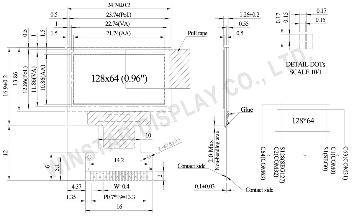
DRAWING
Data source ref: WEO012864VWPP3N0Y000
SPECIFICATIONS
Interface Pin Function
| No. | Symbol | Function | ||||||||
|---|---|---|---|---|---|---|---|---|---|---|
| 1 | C2N | C2P/C2N – Pin for charge pump capacitor; Connect to each other with a capacitor. | ||||||||
| 2 | C2P | |||||||||
| 3 | C1P | C1P/C1N – Pin for charge pump capacitor; Connect to each other with a capacitor. | ||||||||
| 4 | C1N | |||||||||
| 5 | VBAT | Power Supply for DC/DC Converter Circuit This is the power supply pin for the internal buffer of the DC/DC voltage converter. It must be connected to external source when the converter is used. It should be float when the converter is not used. |
||||||||
| 6 | VCC | Power supply for panel driving voltage. This is also the most positive power voltage supply pin. When charge pump is enabled, a capacitor should be connected between this pin and VSS. |
||||||||
| 7 | VSS | Ground of Logic Circuit This is a ground pin. It acts as a reference for the logic pins. It must be connected to external ground. |
||||||||
| 8 | VDD | Power Supply for Logic This is a voltage supply pin. It must be connected to external source. |
||||||||
| 9 | BS0 | Communicating Protocol Select These pins are MCU interface selection input. See the following table:
|
||||||||
| 10 | BS1 | |||||||||
| 11 | CS# | Chip Select This pin is the chip select input. The chip is enabled for MCU communication only when CS# is pulled low. |
||||||||
| 12 | RES# | Power Reset for Controller and Driver This pin is reset signal input. When the pin is low, initialization of the chip is executed. |
||||||||
| 13 | D/C# | In I2C mode, this pin acts as SA0 for slave address selection. When 3-wire serial interface is selected, this pin must be connected to VSS. |
||||||||
| 14~16 | D0~D2 | When serial interface mode is selected, D0 will be the serial clock input: SCLK; D1 will be the serial data input: SDIN. When I2C mode is selected, D2, D1 should be tied together and serve as SDAout, SDAin in application and D0 is the serial clock input, SCL. |
||||||||
| 17 | IREF | Current Reference for Brightness Adjustment This pin is segment current reference pin. A resistor should be connected between this pin and VSS. Set the current lower than 30uA. |
||||||||
| 18 | VCOMH | COM signal deselected voltage level. A capacitor should be connected between this pin and VSS. |
||||||||
| 19 | VCC | Power supply for panel driving voltage. This is also the most positive power voltage supply pin. When charge pump is enabled, a capacitor should be connected between this pin and VSS. |
||||||||
| 20 | VLSS | Ground of Analog Circuit This is an analog ground pin. It should be connected to VSS externally. |
Mechanical Data
| Item | Dimension | Unit |
|---|---|---|
| Dot Matrix | 128 x 64 Dots | - |
| Module dimension | 24.74 x 16.90 x 1.26 | mm |
| Active Area | 21.74 x 10.86 | mm |
| Pixel Size | 0.15 x 0.15 | mm |
| Pixel Pitch | 0.17 x 0.17 | mm |
| Display Mode | Passive Matrix | |
| Display Color | Monochrome | |
| Drive Duty | 1/64 Duty | |
| IC | SSD1315 | |
| Interface | 4-line/3-line SPI, I2C | |
| Size | 0.96 inch | |
Absolute Maximum Ratings
| Parameter | Symbol | Min | Max | Unit |
|---|---|---|---|---|
| Supply Voltage for Logic | VDD | -0.3 | 4.0 | V |
| Charge Pump Regulator | VBAT | -0.3 | 6.0 | V |
| Supply Voltage for Display | VCC | 0 | 18.0 | V |
| Operating Temperature | TOP | -30 | +70 | °C |
| Storage Temperature | TSTG | -30 | +70 | °C |
Electronical Characteristics
DC Electrical Characteristics
| Item | Symbol | Condition | Min | Typ | Max | Unit |
|---|---|---|---|---|---|---|
| Supply Voltage for Logic | VDD | - | 2.8 | 3.0 | 3.3 | V |
| Supply Voltage for Display | VCC | - | 7.0 | 7.5 | 8.0 | V |
| Input High Volt. | VIH | - | 0.8×VDD | - | VDD | V |
| Input Low Volt. | VIL | - | 0 | - | 0.2×VDD | V |
| Output High Volt. | VOH | - | 0.9×VDD | - | VDD | V |
| Output Low Volt. | VOL | - | 0 | - | 0.1×VDD | V |
| Operating Current for VCC (50% display ON) | ICC | - | - | 6 | 12 | mA |
Search keyword: 128x64 oled, oled 128x64, 0.96 oled, 0.96" oled, 0.96 inch oled, oled 0.96, oled 0.96"
