Display Pantalla LCD Display, Pantalla De LCD, Display Para Pantallas LCD
WINSTAR Display - Proveedor de pantallas LCD
WINSTAR ofrece una amplia gama de productos convencionales y diseñados a medida de Displays Industriales, módulos PMOLED y LCM. Nuestras líneas de producción de pantalla LCD display también incluyen Displays LCD Alfanuméricos monocromos TN/STN/FSTN, pantalla LCD gráfica, COG LCD, FSC-LCD, módulos VATN LCM, pantalla TFT LCD, y módulos de pantalla PMOLED. Para dar soporte integral a todos estos productos, nuestro equipo técnico puede ofrecer un soporte completo en una amplia gama de diseños a medida, incluyendo conectores, ZIP, FPC, paneles táctiles, soluciones de conexiones y desarrollo de circuitos electrónicos. El Equipo Técnico de Sistemas Integrados de WINSTAR puede personalizar la placa base y dar soluciones con las pantallas TFT.
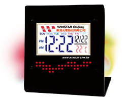
Tipos de display: