

5.2 inch Bar Type TFT LCD
Model No. WF52QSZBSDBN0
►Size : 5.2”
►Resolution : 480 x 128 dots
►View Direction : 6H
►Interface : 8080, MPU
►Controller IC : SSD1963
►Control-Board : Yes
►Brightness (cd/m²): 850
►Frame Through Hole : Yes
►Touch Screen : Without touch screen
►O-Film : Yes
Description
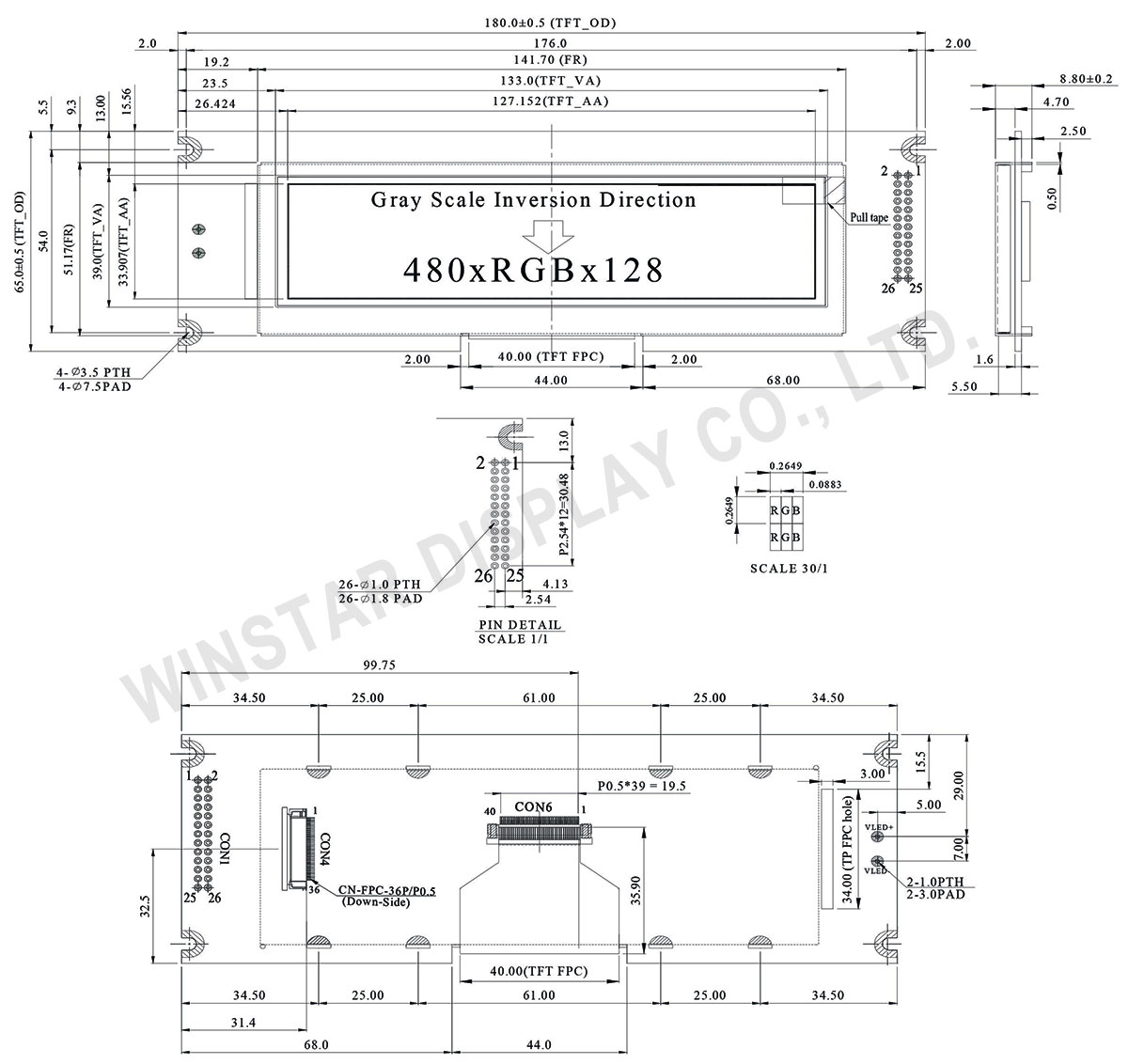
WF52QSZBSDBN0 is a 5.2-inch bar-type TFT LCD with O-film wide viewing angles. The module is built-in with SSD1963 driver IC, supporting 8080 MPU interfaces. It has a resolution of 480×128 dots and a high brightness of 850 cd/m2. The module dimension is 180.0 × 65.0 × 8.8 mm with an active area of 127.152 × 33.9072 mm. The display features a glare surface, 6 o'clock view direction, and 12 o'clock gray scale inversion direction.
The display comes with four screw holes on its PCB board so that users can easily mount it with various applications. The supply voltage for LCM (VCC) is from 3.0V to 3.6V (typical value: 3.3V). This bar TFT can operate at a temperature range from -20℃ to +70℃, and its storage temperatures are from -30℃ to +80℃.
The display comes with four screw holes on its PCB board so that users can easily mount it with various applications. The supply voltage for LCM (VCC) is from 3.0V to 3.6V (typical value: 3.3V). This bar TFT can operate at a temperature range from -20℃ to +70℃, and its storage temperatures are from -30℃ to +80℃.
DRAWING
SPECIFICATIONS
Interface
LCM PIN Definition (CON4)| Pin | Symbol | Function |
|---|---|---|
| 1 | GND | System round pin of the IC. Connect to system ground. |
| 2 | VDD | Power Supply : +3.3V |
| 3 | BL_E | Backlight control signal , H: On \ L: Off |
| 4 | D/C | Data/Command select |
| 5 | WR | Write strobe signal |
| 6 | RD | Read strobe signal |
| 7~14 | DB0~DB7 | Data bus |
| 15~22 | DB8~DB15 | Data bus (When select 8bits mode, this pin is NC) |
| 23~24 | NC | No connect |
| 25 | CS | Chip select |
| 26 | RESET | Hardware reset |
| 27 | LR | Right /Left selection; Default R/L is Pull High |
| 28 | UD | Up/down selection; Default U/D is Pull High |
| 29~32 | NC | No connection |
| 33~34 | VLED- | VLED- for B/L LED inverter (GND) |
| 35~36 | VLED+ | VLED+ for B/L LED inverter (+5V) |
LCM PIN Definition (CON1)
| Pin | Symbol | Function |
|---|---|---|
| 1 | NC(FG) | No connect (Frame Grand) |
| 2 | GND | System round pin of the IC. Connect to system ground. |
| 3 | VDD | Power Supply : +3.3V |
| 4 | BLE | Backlight control signal , H: On \ L: Off |
| 5 | WR | Write strobe signal |
| 6 | RD | Read strobe signal |
| 7 | CS | Chip select |
| 8 | D/C | Data/Command select |
| 9 | NC | No connect |
| 10 | RESET | Hardware reset |
| 11~18 | DB0~DB7 | Data bus |
| 19~20 | NC | No connect |
| 21 | VLED+ | VLED+ for B/L LED inverter (+5V) |
| 22 | VLED- | VLED- for B/L LED inverter (GND) |
| 23~25 | NC | No connect |
| 26 | GND | Hardware reset |
General Specifications
| Item | Dimension | Unit |
|---|---|---|
| Size | 5.2 | inch |
| Dot Matrix | 480 × RGB × 128 | dots |
| Module dimension | 180.0 × 65.0 × 8.8 | mm |
| Active area | 127.152 × 33.9072 | mm |
| Dot pitch | 0.0883 × 0.2649 | mm |
| LCD type | TFT, Normally White, Transmissive | |
| View Direction | 6 o'clock | |
| Gray Scale Inversion Direction | 12 o'clock | |
| Aspect Ratio | Bar Type | |
| Backlight Type | LED, Normally White | |
| Controller IC | SSD1963 | |
| Interface | Digital 8080 family MPU 8bit/16bit | |
| With /Without TP | Without touch panel (screen) | |
| Surface | Glare | |
Absolute Maximum Ratings
| Item | Symbol | Min | Typ | Max | Unit |
|---|---|---|---|---|---|
| Operating Temperature | TOP | -20 | - | +70 | ℃ |
| Storage Temperature | TST | -30 | - | +80 | ℃ |
Electrical Characteristics
| Item | Symbol | Condition | Min | Typ | Max | Unit |
|---|---|---|---|---|---|---|
| Supply Voltage For LCM | VDD | - | 3.0 | 3.1 | 3.3 | V |
| Supply Current For LCM | IDD | - | - | 200 | - | mA |
Search keyword: tft 5.2, tft 5.2", 5.2 tft lcd, 5.2" tft lcd, 5.2 inch tft lcd, tft lcd 5.2, 5.2 tft display, 5.2" tft display, 5.2 inch tft display, tft display 5.2, tft display 5.2",bar type tft
