


Chip on Glass LCD Module 240x128 with PCB
Model No. WO240128B2
►COG LCD
►Graphic LCD
►240 x 128 dots
►IC: ST7586S
►3.3V power supply
►1/128 duty cycle
►Interface : Default 6800, Option 8080, SPI-4 Line/SPI-3Line 9bit
Description
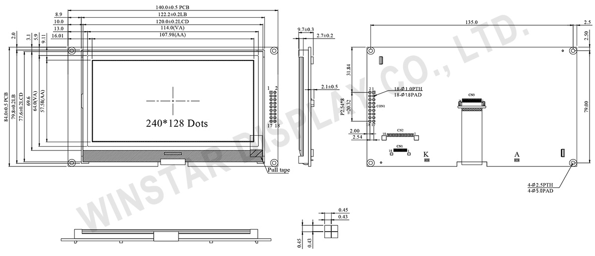
The WO240128B2 model is a COG LCD display, an enhanced version of the WO240128B model, featuring a PCB board on the module and a resolution of 240x128 dots. The module has dimensions of 140.0 × 84.0 mm, with an active area size measuring 107.98 × 57.58 mm. It incorporates the ST7586S controller IC, supporting a default 6800 8-bit interface, with optional 8080 8-bit parallel and serial SPI interfaces. The power supply voltage is 3.3V, and it operates with a 1/128 duty and 1/12 bias.
The WO240128B2 offers the advantage of a circuit layout on the PCB board, along with screw holes for easy integration into customers' applications. Additionally, it provides flexibility with three connector pitch sizes: 2.54mm (default), 1.0mm, and 0.5mm. There's also the option for a VDD 5V power supply voltage.
This module is designed to operate within a temperature range of -20℃ to +70℃, with storage temperatures ranging from -30℃ to +80℃. Its versatility makes it suitable for various applications, including home appliances, control systems, industrial devices, and testing equipment.
The WO240128B2 is equipped with FSTN positive Transflective technology and features a white LED backlight. For different LCD types or LED combinations, please feel free to contact us.
If you have any further questions or need additional information, please don't hesitate to ask.
DRAWING
SPECIFICATIONS
Interface Pin Function
| Pin No. | Symbol | Description |
| 1 | VDD | Power supply |
| 2 | NC | No connection |
| 3 | VSS | Ground |
| 4 | CSB | Chip select input pin CSB=“L”: This chip is selected and the MPU interface is active CSB=“H”: This chip is not selected and the MPU interface is disabled (D[7:0] are high impedance) |
| 5 | RSTB | Reset input pin. When RSTB is “L”, internal initialization procedure is executed |
| 6 | E | Read / Write control input pin. R/W = “H”: When E is “H”, data bus is in output status. R/W = “L”: The data are latched at the falling edge of the E signal. |
| 7~14 | D7~D0 | The bi-directional data bus of the MPU interface. When CSB is “H”, they are high impedance |
| 15 | R/W | Read / Write control input pin R/W = “H” : read R/W = “L” : write |
| 16 | A0 | The function of this pin is different in parallel and serial interface In parallel interface: A0 is register selection input A0 = "H": inputs on data bus are display data A0 = "L": inputs on data bus are command |
| 17 | A | LED+ |
| 18 | K | LED- |
Mechanical Data
| Item | Dimension | Unit |
|---|---|---|
| Number of dots | 240 × 128 | - |
| Module dimension | 140.0 × 84.0 × 9.7 | mm |
| View area | 114.0 × 64.0 | mm |
| Active area | 107.98 × 57.58 | mm |
| Dot size | 0.43 × 0.43 | mm |
| Dot pitch | 0.45 × 0.45 | mm |
| Drive Method | 1/128 Duty,1/12 Bias | |
| Backlight Type | LED | |
| IC | ST7586S | |
| Interface | 6800 | |
Absolute Maximum Ratings
| Item | Symbol | Min | Typ | Max | Unit |
|---|---|---|---|---|---|
| Operating Temperature | TOP | -20 | - | +70 | ℃ |
| Storage Temperature | TST | -30 | - | +80 | ℃ |
| Digital Power Supply Voltage | VDDI | -0.3 | - | 3.6 | V |
| Analog Power supply voltage | VDDA | -0.3 | - | 3.6 | V |
| LCD Power supply voltage | V0-XV0 | -0.3 | - | 19 | V |
| LCD Power supply voltage | VG | -0.3 | - | 5.5 | V |
Electrical Characteristics
| Item | Symbol | Condition | Min | Typ | Max | Unit |
|---|---|---|---|---|---|---|
| Supply Voltage For Logic | VDD-VSS | - | 3.0 | 3.3 | 3.6 | V |
| Supply Voltage For LCM | VOP | Ta=-20℃ Ta=25℃ Ta=+70℃ |
- 14.8 - |
- 15.0 - |
- 15.2 - |
V V V |
| Input High Volt. | VIH | - | 0.7VDD | - | VDD | V |
| Input Low Volt. | VIL | - | VSS | - | 0.3 VDD | V |
| Output High Volt. | VOH | - | 0.8 VDD | - | VDD | V |
| Output Low Volt. | VOL | - | VSS | - | 0.2VDD | V |
| Supply Current | IDD | VDD=3.3V | - | 2.0 | 4.0 | mA |
Search keyword: 240x128 lcd, 240 x 128 lcd, lcd 240x128, lcd 240 x 128
