


1.71 inch 128x32 COG Graphic OLED Module
Model No. WEO012832P
►Small OLED Display, Smallest OLED
►Suitable for wearable device
►Type: Graphic
►Structure: COG
►Size: 1.71 inch
►128 x 32 Dot Matrix
►IC:CH1115
►3V Power supply
►1/32 duty
►Interface: SPI, I2C
►Display Color: White / Yellow
Description
WEO012832P is a 1.71-inch COG small OLED display module that is made of 128x32 dots. This module is built in with CH1115 IC; it supports I2C and SPI interface, 3V power supply, 1/32 driving duty, the supply voltage of logic is 3.0V (VDD), and the current with 50% checkerboard display is 5mA @ 12V VCC (for white color). The WEO012832P model is an IC alternative solution to the WEO012832G model; the mechanical size and PFC pin definition are the same. For more details, please check the datasheet.
The WEO012832P is a COG structure OLED display that is ultra-thin and has no need for backlight; it's lightweight and has low power consumption. This 1.71-inch small OLED module is suitable for smart home applications, portable devices, health devices, testing instruments, etc. WEO012832P can be operated at temperatures from -40℃ to +80℃; its storage temperatures range from -40℃ to +85℃.
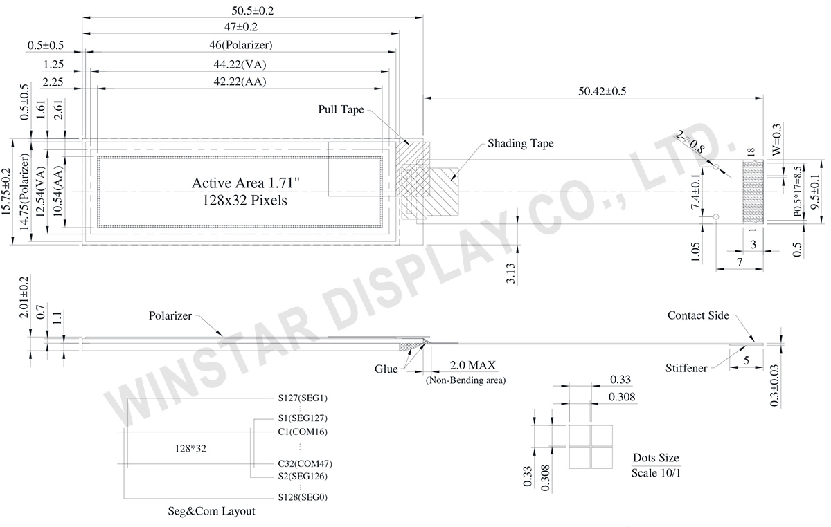
DRAWING
Data source ref: WEO012832PWAP3N00000
SPECIFICATIONS
Interface Pin Function
| No. | Symbol | Function | ||||||||||||
|---|---|---|---|---|---|---|---|---|---|---|---|---|---|---|
| 1 | ESD_GND | ESD Ground pin | ||||||||||||
| 2 | VPP | OLED panel power supply. | ||||||||||||
| 3 | VSS | This is a ground pin. | ||||||||||||
| 4 | VSS | This is a ground pin. | ||||||||||||
| 5 | VDD | Power Supply for Logic | ||||||||||||
| 6 | __ CS |
This pad is the chip select input. When /CS = “L”, then the chip select becomes active, and data/command I/O is enabled. | ||||||||||||
| 7 | ___ RES |
This is a reset signal input pad. When /RES is set to “L”, the settings are initialized. The reset operation is performed by the /RES signal level. | ||||||||||||
| 8 | A0 | This is the Data/Command control pad that determines whether the data bits are data or a command. In I2C interface, this pad serves as SA0 to distinguish the different address of OLED driver. |
||||||||||||
| 9 | SCL | The serial clock input pad | ||||||||||||
| 10 | SI/SDA | The serial data input pad | ||||||||||||
| 11 | NC | Dummy Pin | ||||||||||||
| 12 | IREF | This is a segment current reference pad. A resistor should be connected between this pad and VSS. Set the current at 18.75μA. | ||||||||||||
| 13 | VCOMH | The pin is for COM signal deselected voltage level. A capacitor should be connected between this pin and VSS. |
||||||||||||
| 14 | VPP | OLED panel power supply. | ||||||||||||
| 15 | IM0 | These are the MPU interface mode select pads.
|
||||||||||||
| 16 | IM1 | |||||||||||||
| 17 | VSS | This is a ground pin. | ||||||||||||
| 18 | ESD_GND | ESD Ground pin |
Mechanical Data
| Item | Dimension | Unit |
|---|---|---|
| Dot Matrix | 128 × 32 | Dots |
| Module dimension | 50.50 × 15.75 × 2.01 | mm |
| Active Area | 42.22 × 10.54 | mm |
| Pixel Size | 0.308 × 0.308 | mm |
| Pixel Pitch | 0.33 × 0.33 | mm |
| Display Mode | Passive Matrix | |
| Display Color | Monochrome | |
| Drive Duty | 1/32 Duty | |
| IC | CH1115 | |
| Interface | SPI, I2C | |
| Size | 1.71 inch | |
Absolute Maximum Ratings
| Parameter | Symbol | Min | Max | Unit |
|---|---|---|---|---|
| Supply Voltage for Logic | VDD | -0.3 | 3.6 | V |
| Supply Voltage for Display | VPP | -0.3 | 14.5 | V |
| Operating Temperature | TOP | -40 | +80 | °C |
| Storage Temperature | TSTG | -40 | +85 | °C |
Electronical Characteristics
| Item | Symbol | Condition | Min | Typ | Max | Unit |
|---|---|---|---|---|---|---|
| Supply Voltage for Logic | VDD | - | 1.65 | 3.0 | 3.3 | V |
| Supply Voltage for Display | VPP | - | 6.4 | 12.0 | 12.5 | V |
| High Level Input | VIH | - | 0.8×VDD | - | VDD | V |
| Low Level Input | VIL | - | VSS | - | 0.2×VDD | V |
| High Level Output | VOH | - | 0.8×VDD | - | VDD | V |
| Low Level Output | VOL | - | VSS | - | 0.2×VDD | V |
| Display 50% Pixel on | IPP | VPP=12V | - | 5 | 10 | mA |
Search keyword: 128x32 oled, oled 128x32, 1.71 oled, 1.71" oled, 1.71 inch oled, oled 1.71, oled 1.71"
