

LCD COG Module 240x64
Model No. WO24064A1
►COG Display LCD
►Graphic LCD
►240 x 64 dots
►IC: ST7565P
►3.3V power supply
►Interface : 6800/8080/SPI
DRAWING
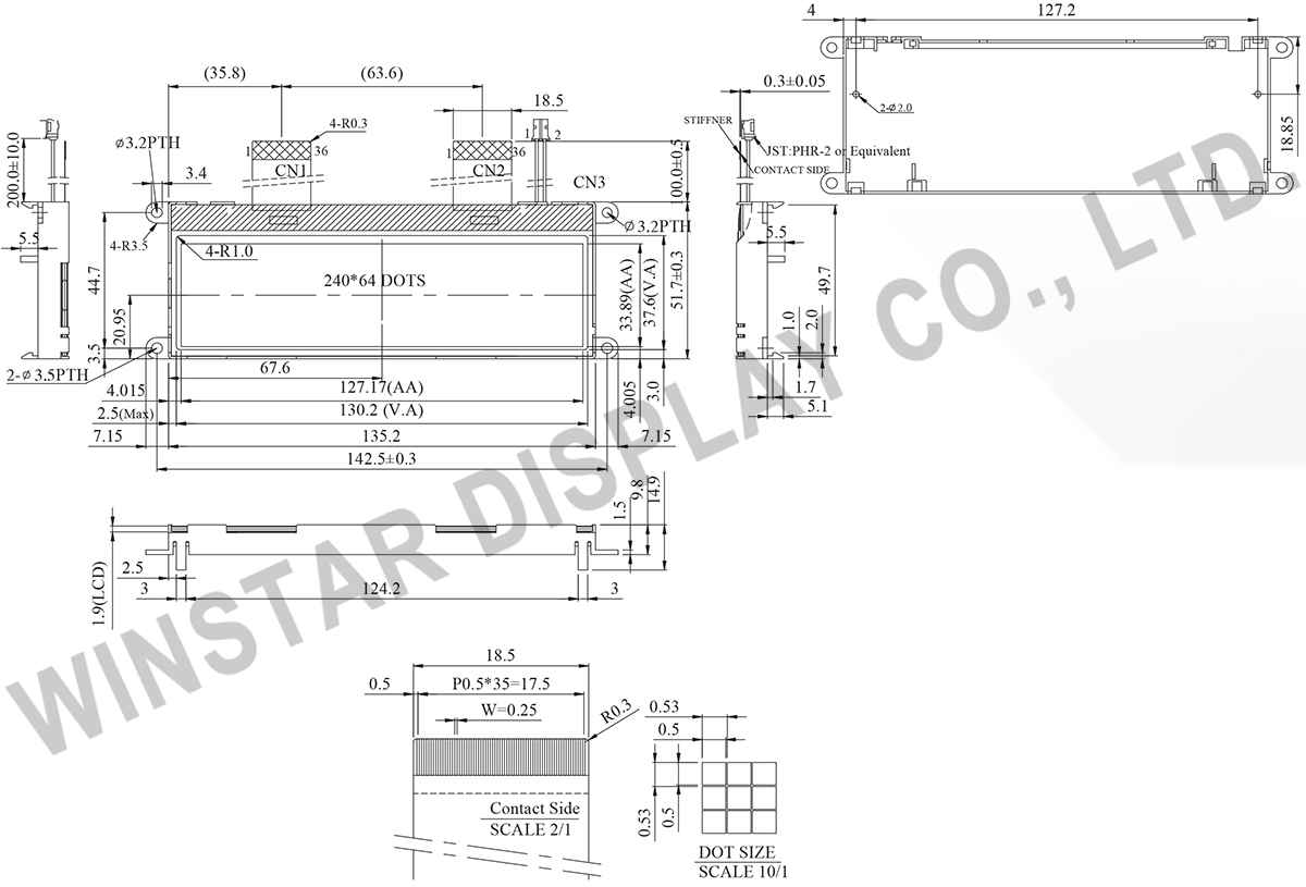
Data source ref:WO24064A1-TFH#
SPECIFICATIONS
Interface Pin Function
| Pin No. | Symbol | Level | Description |
|---|---|---|---|
| 1 | NC | No connection | |
| 2 | FR | O | This is the liquid crystal alternating current signal terminal. |
| 3 | CL | I/O | This is the display clock input terminal The following is true depending on the M/S and CLS status. |
| 4 | /DOF | O | This is the LCD blanking control terminal. |
| 5 | /CS1 | I | This is the chip select signal. When /CS1 = “L” and CS2 = “H”, then the chip Select becomes active, and data/command I/O is enabled. |
| 6 | CS2 | I | |
| 7 | /RES | I | When /RES is set to “L”, the register settings are initialized (cleared). The reset operation is performed by the /RES signal level. |
| 8 | A0 | I | This is connect to the least significant bit of the normal MPU address bus, and it determines whether the data bits are data or command. A0 = “H”: Indicates that D0 to D7 are display data. A0 = “L”: Indicates that D0 to D7 are control data. |
| 9 | /WR | I | When connected to 8080 series MPU, this pin is treated as the “/WR” signal of the 8080 MPU and is LOW-active. The signals on the data bus are latched at the rising edge of the /WR signal. When connected to 6800 series MPU, this pin is treated as the “R/W” signal of the 6800 MPU and decides the access type : When R/W = “H”: Read. When R/W = “L”: Write. |
| 10 | /RD | I | When connected to 8080 series MPU, this pin is treated as the “/RD” signal of the 8080 MPU and is LOW-active. The data bus is in an output status when this signal is “L”. When connected to 6800 series MPU, this pin is treated as the “E” signal of the 6800 MPU and is HIGH-active. This is the enable clock input terminal of the 6800 Series MPU. |
| 11~18 | DB0~DB7 | I/O | Data bus |
| 19 | VDD | P | Power supply |
| 20 | VSS | P | Ground |
| 21 | Vout | O | DC/DC voltage converter. Connect a capacitor between this terminal and VSS or VDD |
| 22 | C3+ | O | DC/DC voltage converter |
| 23 | C1- | ||
| 24 | C1+ | ||
| 25 | C2+ | ||
| 26 | C2- | ||
27 |
V4 | P | This is a multi-level power supply for the liquid crystal drive. The voltage Supply applied is determined by the liquid crystal cell, and is changed through the use of a resistive voltage divided or through changing the impedance using an op. amp. Voltage levels are determined based on Vss, and must maintain the relative magnitudes shown below. V0 ≧V1 ≧V2 ≧V3 ≧V4 ≧Vss |
| 28 | V3 | ||
| 29 | V2 | ||
| 30 | V1 | ||
| 31 | V0 | ||
| 32 | VR | I | Output voltage regulator terminal. Provides the voltage between VSS and V0 through a resistive voltage divider. IRS = “L” : the V0 voltage regulator internal resistors are not used. IRS = “H” : the V0 voltage regulator internal resistors are used. |
| 33 | C86 | I | This is the MPU interface selection pin. C86 = “H”: 6800 Series MPU interface. C86 = “L”: 8080 Series MPU interface. |
| 34 | P/S | I | This pin configures the interface to be parallel mode or serial mode. P/S = “H”: Parallel data input/output. P/S = “L”: Serial data input. The following applies depending on the P/S status: P/S Data/Command Data Read/Write Serial Clock “H” A0 D0 to D7 /RD, /WR X “L” A0 SI (D7) Write only SCL (D6) When P/S = “L”, D0 to D5 must be fixed to “H”. /RD (E) and /WR (R/W) are fixed to either “H” or “L”. The serial access mode does NOT support read operation. |
| 35 | NC | No connection | |
| 36 | NC | No connection |
Mechanical Data
| Item | Dimension | Unit |
|---|---|---|
| Number of Dots | 240 x 64 | - |
| Module dimension | 142.5 x 51.7 x 14.9(MAX) | mm |
| View area | 130.2 x 37.6 | mm |
| Active area | 127.17 x 33.89 | mm |
| Dot size | 0.50 x 0.50 | mm |
| Dot pitch | 0.53 x 0.53 | mm |
| Duty | 1/65 | |
| Backlight Type | LED | |
| IC | ST7565P | |
| Interface | 6800/8080/4-Line SPI | |
Absolute Maximum Ratings
| Item | Symbol | Min | Typ | Max | Unit |
|---|---|---|---|---|---|
| Operating Temperature | TOP | -20 | - | +70 | ℃ |
| Storage Temperature | TST | -30 | - | +80 | ℃ |
| Power Supply Voltage | VDD | -0.3 | - | 3.6 | V |
| Power supply voltage (VDD standard) | V0,VOUT | -0.3 | - | 14.5 | V |
| Power supply voltage (VDD standard) | V1,V2,V3,V4 | -0.3 | - | V0+0.3 | V |
Electrical Characteristics
| Item | Symbol | Condition | Min | Typ | Max | Unit |
|---|---|---|---|---|---|---|
| Supply Voltage For Logic | VDD-VSS | - | 3.0 | 3.3 | 3.6 | V |
| Supply Voltage For LCM | V0-VSS | Ta=-20℃ Ta=25℃ Ta=70℃ |
- 10. - |
- 11.0 - |
- 11.3 - |
V V V |
| Input High Volt. | VIH | - | 0.8 VDD | - | VDD | V |
| Input Low Volt. | VIL | - | VSS | - | 0.2VDD | V |
| Output High Volt. | VOH | - | 0.8VDD | - | VDD | V |
| Output Low Volt. | VOL | - | VSS | - | 0.2VDD | V |
| Supply Current(No include LED Backlight) | IDD | VDD=3.3V | - | 1.5 | 2.5 | mA |
Search Keyword: lcd 240x64, lcd 240 x 64, 240x64 lcd, 240 x 64 lcd
